

High pressure P-shaped metal oxide semiconductor tube of silicon-on-insulator
A technology of silicon-on-insulator and semiconductor tube, applied in the field of power semiconductor devices, can solve the problems of transistor burning, increase chip area consumption, reduce chip usage area, etc., and achieve the effect of preventing burning
- Summary
- Abstract
- Description
- Claims
- Application Information
AI Technical Summary
Problems solved by technology
Method used
Image

Examples
Embodiment Construction
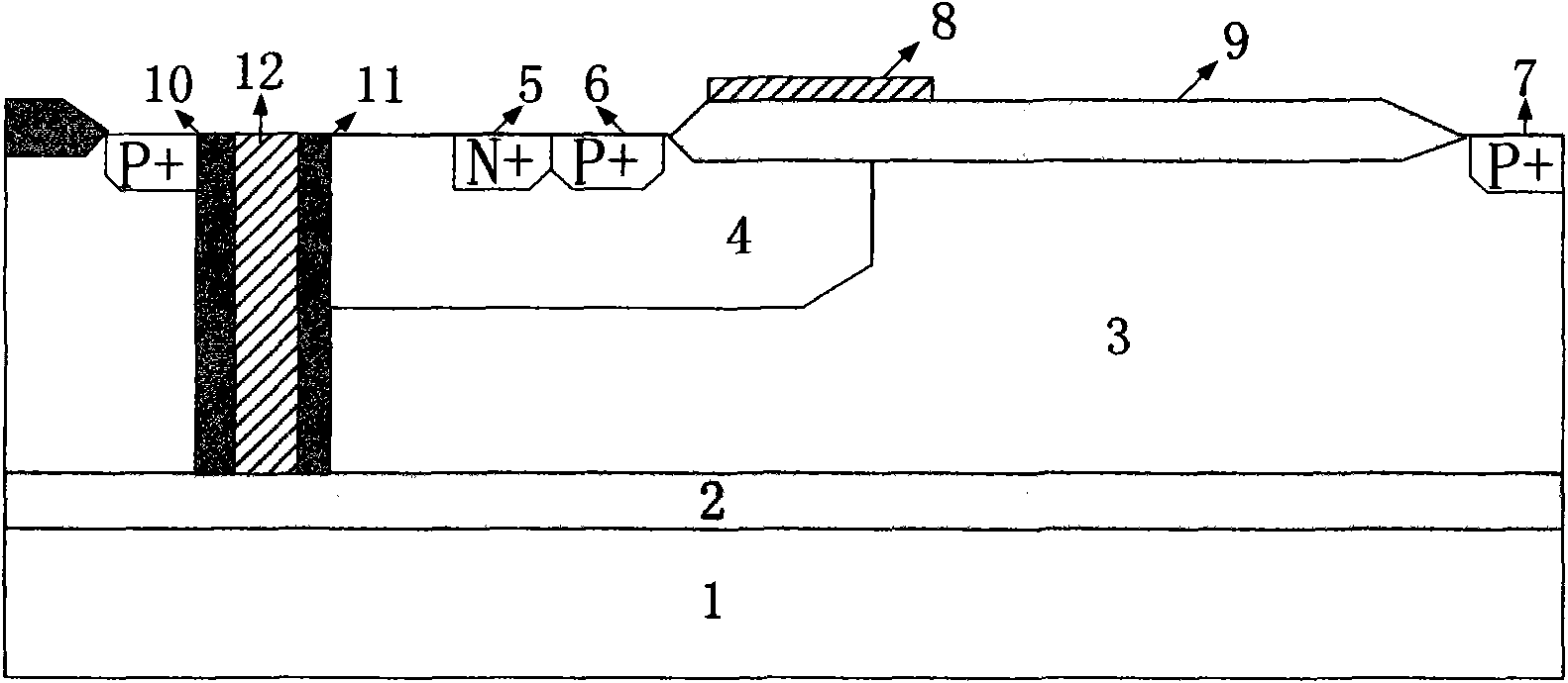
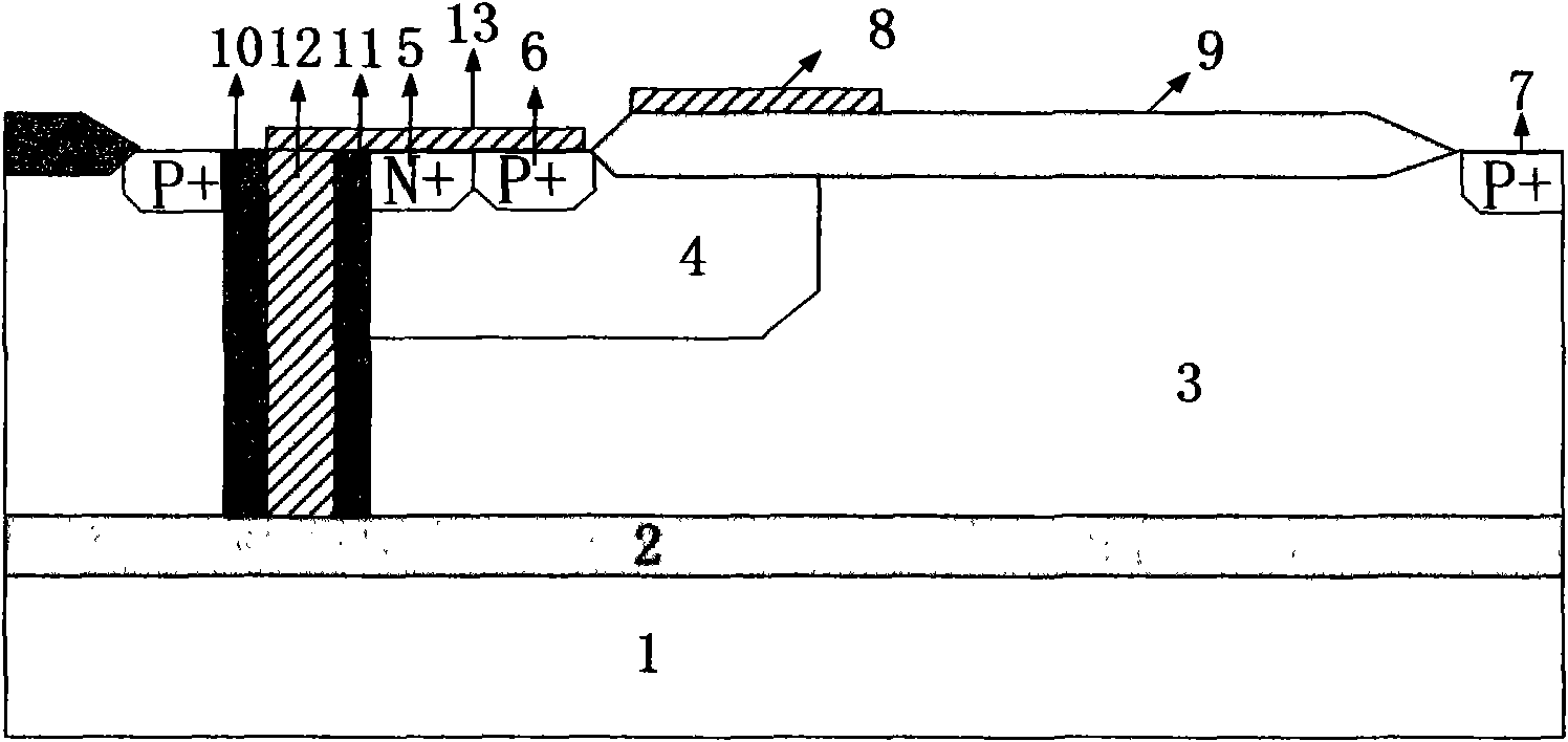
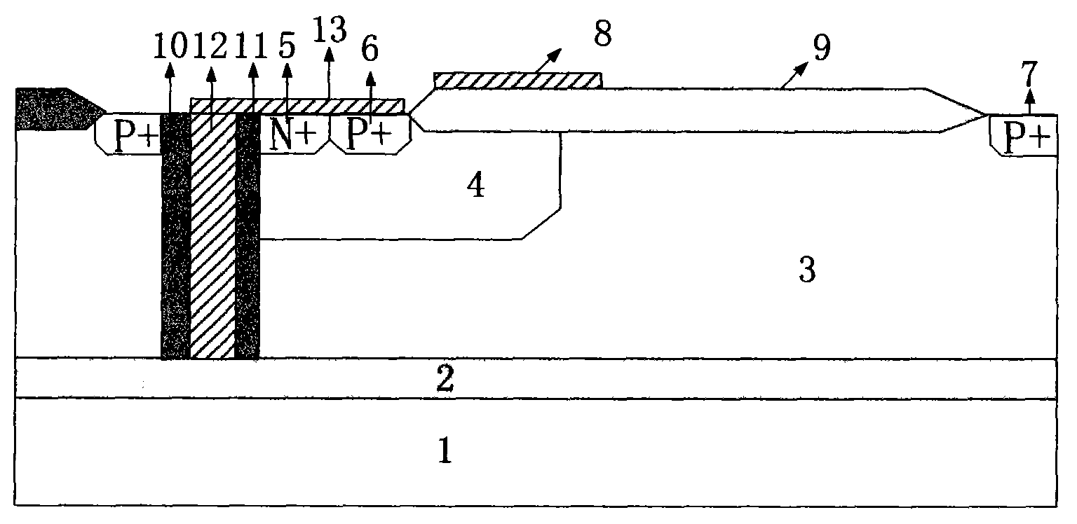
[0016] Please refer to figure 2 , a high-voltage P-type metal oxide semiconductor transistor for silicon-on-insulator, comprising: a semiconductor substrate 1, a buried oxide layer 2 is arranged on the semiconductor substrate 1, and a left oxide layer 10 is arranged on the buried oxide layer 2 , the right oxide layer 11 and the polysilicon layer 12 between the left oxide layer 10 and the right oxide layer 11 constitute an isolation deep groove, and the left and right sides of the isolation deep groove are all high-voltage P-type metal oxide semiconductor transistors of silicon-on-insulator with a traditional structure The high-voltage P-type metal oxide semiconductor transistor of this silicon-on-insulator is composed as follows: a P-type semiconductor drift region 3 is arranged on the buried oxide layer 2, and an N-type well 4 and a P-type semiconductor drift region 3 are arranged on the P-type semiconductor drift region 3. The drain region 7 is provided with an N-type conta...
PUM
 Abstract
Description
Claims
Application Information