Organic electroluminescent device

An electroluminescence display and luminescence technology, which is applied in the direction of electric solid-state devices, electrical components, semiconductor devices, etc., can solve the problems that the slope area is easy to be blown, increase cost, consume, etc., achieve obvious effect and reduce the probability of circuit breaker , Improve the effect of product yield

Active Publication Date: 2010-04-07
KUNSHAN VISIONOX DISPLAY TECH +2
View PDF0 Cites 8 Cited by
  • Summary
  • Abstract
  • Description
  • Claims
  • Application Information

AI Technical Summary

Problems solved by technology

Therefore, these slopes are weak areas in the overlapping area. When the current is too large, the slope area is easy to be fused, causing the second electrode material in the via hole to be separated from the surrounding second electrode material, thereby causing an open circuit, resulting in Hidden line
[0007] For the OLED light source, due to the large current, usually 0.1~1A or even larger, it is easier to cause an open circuit due to the burning of the weak area on the slope, so that the entire light source cannot emit light
[0008] If the weak area is prevented from being blown by increasing the thickness of the second electrode material, more material and evaporation time will be consumed, which will increase the cost

Method used


Image

  • Organic electroluminescent device
  • Organic electroluminescent device
  • Organic electroluminescent device

Examples


Embodiment 1

[0044] Embodiment 1 is an OLED display device, and its preparation method is as follows:

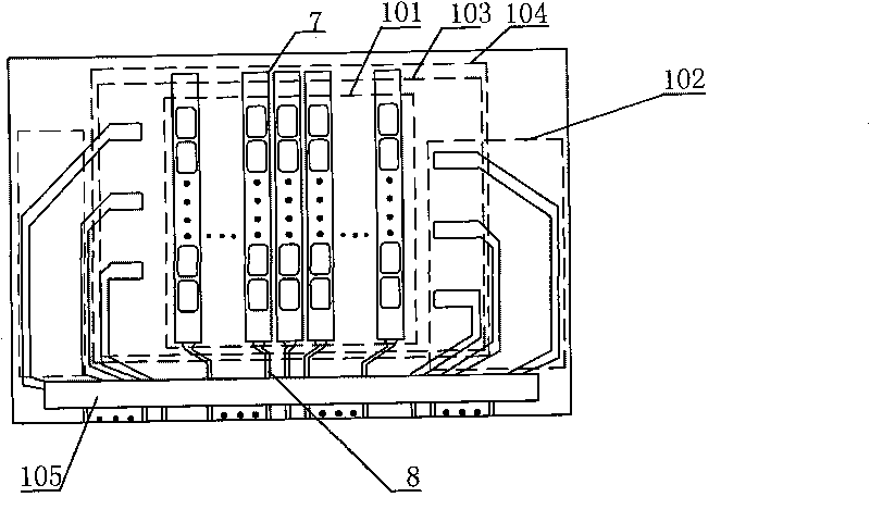
[0045] (1) Sputter the entire layer of ITO5 on the glass substrate 4 . Part of the ITO pattern after photolithography is used as the first electrode 7 and the first electrode lead 8 of the light emitting region 101 , and the other part is used as the second electrode lead of the second electrode lead region 102 .

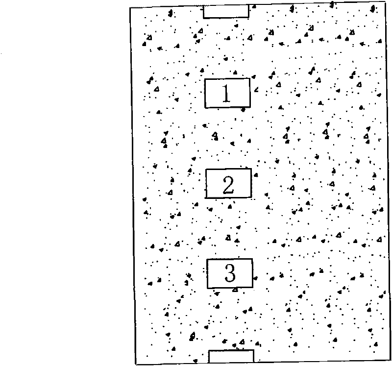
[0046] (2) Prepare an insulating layer and a spacer column (not shown) by photolithography, which is a necessary process for realizing RGB color, and different pixels are separated to realize a pixel array. The covering area of ​​the insulating layer material is 104, and rectangular through holes 1a, 1b, 2a, 2b, 3a, 3b, etc. are formed between the insulating layer materials in the overlapping areas.

[0047] (3) The organic electroluminescence material is deposited by vacuum evaporation method to form the organic functional layer 14, including the hole injection layer 9, the ...

Embodiment 2

[0054] The difference between embodiment 2 and comparative example 1 is in steps (1) and (2):

[0055] (1) On the glass substrate 4, the whole layer of ITO5 and chromium 6 is sputtered. The pattern of chromium is etched first, and then the pattern of ITO is etched. Part of the photoetched ITO and chromium pattern is used as the first electrode and the first electrode lead of the light emitting region 101 , and the other part is used as the electrode lead of the second electrode lead region 102 .

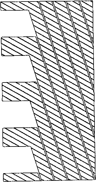
[0056] (2) Prepare an insulating layer and isolation posts (not shown) by photolithography. Such as Figure 8 As shown, each lead wire of the second electrode overlaps with the second electrode through four rectangular through holes between the insulating layers.

Embodiment 3

[0058] The difference between embodiment 3 and comparative example 1 is in steps (1) and (2):

[0059] (1) Sputter ITO5 on the position of the light-emitting area on the glass substrate. Molybdenum, aluminum, and molybdenum materials are sequentially sputtered in the second electrode lead area to form a three-layer structure of molybdenum / aluminum / molybdenum. The ITO pattern of the light-emitting area 101 is firstly etched to serve as the first electrode and the first electrode lead; and then the second electrode lead area 102 is etched to form the molybdenum / aluminum / molybdenum pattern as the second electrode lead.

[0060] (2) Prepare an insulating layer and isolation posts (not shown) by photolithography. Such as Figure 9 As shown, each lead wire of the second electrode overlaps with the second electrode through two circular through holes between the insulating layers.


PUM


Abstract

The invention discloses an organic electroluminescent device, and relates to an OLED display device and an OLED light source, in particular to a connecting mode of a second electrode and a lead thereof of the OLED display device and the OLED light source. A through hole for lapping the lead of each second electrode and the second electrode is one in the prior art, due to the problems of deposition angles and the like, the second electrode material on a slope at the periphery of the through hole is less, and the lead of the second electrode is easy to blow so as to appear a concealed wire. The through hole is multiple, and has common shapes such as rectangle, circle, oval and the like. Because the lapping area is increased, the blowing probability is decreased; and the electrical conductivity of the through hole is increased, inconsistent resistance is improved, and the luminescence of a whole screen body is more uniform.

Description

technical field [0001] The present invention relates to an organic electroluminescent device (Organic Light Emitting Diode, hereinafter referred to as OLED), in particular to a connection method between a second electrode of an OLED display device or an OLED light source and its lead. Background technique [0002] OLED is a display device made of the phenomenon that carriers enter the organic functional layer to recombine under the action of an electric field from the first electrode (usually the anode) and the second electrode (usually the cathode) to emit light. Compared with LCD, OLED has the advantages of all solid state, no need for backlight, high contrast, ultra-thin, and flexible display. OLED can be made into a dot matrix screen to dynamically display images, and can also be used as a light source. [0003] For OLED display devices, the light-emitting region has a first electrode, an organic functional layer, and a second electrode. Under the action of an electric ...

Claims


Application Information

Patent Timeline
Patent Type & Authority Applications(China)
IPC IPC(8): H01L27/32H01L23/528H01L51/52
Inventor 邱勇李旺生
Owner KUNSHAN VISIONOX DISPLAY TECH
Why Eureka
Try Eureka