Thin film transistor liquid crystal display array substrate and manufacturing method thereof

A thin-film transistor and liquid crystal display technology, which is applied in semiconductor/solid-state device manufacturing, instruments, electrical components, etc., can solve the problems of easy breakpoints in signal lines and poor TFT-LCD array substrates, etc., to reduce the chance of drilling, The effect of reducing the slope angle and reducing the probability of signal line disconnection

Active Publication Date: 2014-03-12
BOE TECH GRP CO LTD +1
View PDF2 Cites 0 Cited by
  • Summary
  • Abstract
  • Description
  • Claims
  • Application Information

AI Technical Summary

Problems solved by technology

[0007] It can be seen that in the TFT-LCD array substrate produced by the existing four-step patterning process, the signal line is prone to have breakpoints in the crossing area with the gate line or the common electrode line, resulting in a bad TFT-LCD array substrate.

Method used


Image

  • Thin film transistor liquid crystal display array substrate and manufacturing method thereof
  • Thin film transistor liquid crystal display array substrate and manufacturing method thereof
  • Thin film transistor liquid crystal display array substrate and manufacturing method thereof

Examples


Embodiment 1

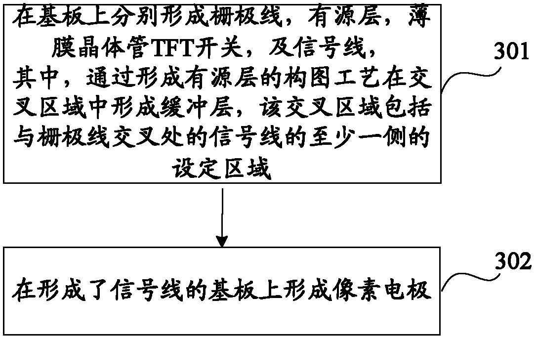
[0046] Embodiment 1. In this embodiment, forming a TFT-LCD array substrate through four patterning processes includes: forming gate lines on the substrate through the first patterning process. The substrate of the TFT-LCD array substrate is generally a glass substrate. , Using sputtering or thermal evaporation method to deposit a layer of gate metal layer on the substrate, then, after applying photoresist on the gate metal layer, the photoresist is exposed through a mask with gate line patterns , Development, and formation of gate lines through processes such as etching and stripping. Here, the etching is wet etching, and the metal that is not covered by the photoresist is etched away by the chemical solution. The material of the gate metal layer includes one or more of Al, Mo, Cu, MoW, and Cr.

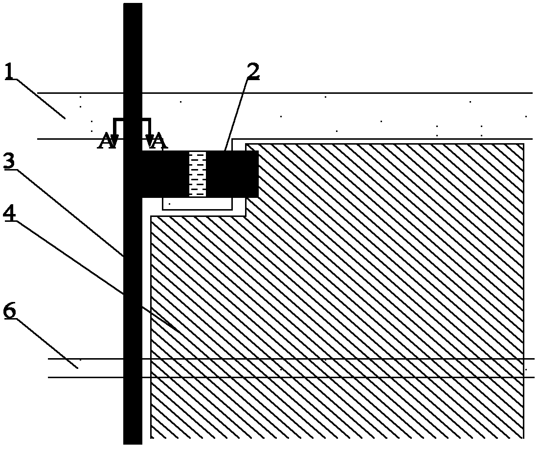
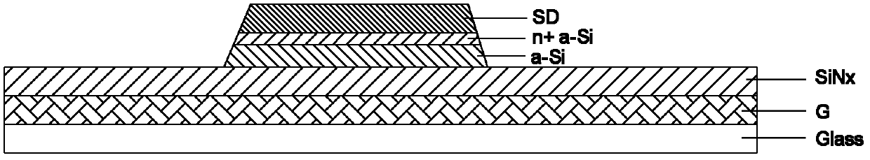
[0047] The active layer, the thin film transistor TFT switch, and the signal line are formed on the substrate on which the gate line is formed through the second patterning process. Amo...

Embodiment 2

[0071] Embodiment 2. In this embodiment, forming a TFT-LCD array substrate through five patterning processes includes: forming gate lines on the substrate through the first patterning process; depositing a semiconductor layer and doping on the substrate where the gate lines are formed. In the hetero semiconductor layer, the active layer and the TFT channel are formed by the second patterning process; the signal lines and the TFT source and drain electrodes are formed on the substrate with the TFT channel formed by the third patterning process; and the TFT source and drain electrodes are formed by the fourth patterning process The process forms a passivation layer and a passivation layer via hole is formed on the drain electrode of the TFT switch; finally, the pixel electrode is formed through the fifth patterning process, and the pixel electrode is connected to the drain electrode of the TFT switch through the via hole. Wherein, a buffer layer is formed in the intersection area ...


PUM

PropertyMeasurementUnit
transmittivityaaaaaaaaaa

Abstract

Disclosed in the invention are a thin film transistor liquid crystal display (TFT-LCD) array substrate and a manufacturing method thereof, thereby reducing an unqualified rate of a TFT-LCD array substrate. The manufacturing method comprises: respectively forming a gate line, an active layer, a thin film transistor (TFT) switch and a signal line on a substrate and forming buffer layers in intersection regions by utilizing a composition process for forming the active layer, wherein the intersection regions include a set region at at least one side of the signal line at the position of intersection with the gate line; and forming a pixel electrode on the substrate, wherein the signal line has been formed on the substrate.

Description

Technical field [0001] The invention relates to the technical field of liquid crystal displays, in particular to a thin film transistor liquid crystal display array substrate and a manufacturing method. Background technique [0002] In recent years, with the advancement of science and technology, digital television has begun to enter daily life. Thin Firm Transistor Liquid Crystal Display (TFT-LCD) has become the current leading product due to its small size, low power consumption, no radiation, and high resolution. [0003] The TFT-LCD is mainly composed of an array substrate and a color film substrate in a pair of boxes. Among them, the production process of the TFT-LCD array substrate determines its product performance, yield and price. [0004] At present, the TFT-LCD array substrate is completed through multiple patterning processes. Each patterning process includes: masking, exposure, development, etching, and stripping. Among them, the etching process includes dry etching and...

Claims


Application Information

Patent Timeline
Patent Type & Authority Patents(China)
IPC IPC(8): H01L21/77G02F1/1362G02F1/1368
Inventor 沈奇雨郭建王玲杰朱朋举王德帅
Owner BOE TECH GRP CO LTD
Why Eureka
Try Eureka