

Gating method of memory and circuit structure implementing same
A memory and gating technology, applied in the field of micro-nano electronics, which can solve problems such as crosstalk power consumption
- Summary
- Abstract
- Description
- Claims
- Application Information
AI Technical Summary
Problems solved by technology
Method used
Image

Examples
Embodiment Construction
[0059] The invention is described more fully below with reference to the drawings, which provide preferred embodiments but should not be considered limited to the embodiments set forth herein.
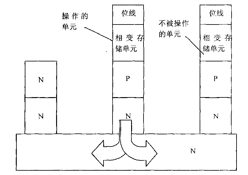
[0060] In the phase-change memory to realize the address selection process, the diode is used as the selection tube. The diode can be: a polycrystalline or single crystal diode, a Schottky diode, a gate-source (or gate-drain) connected field effect transistor, a gate-source (or gate-drain) connected MOSFET, a Zener diode, or Silicon-controlled diodes, P-I-N structure diodes, etc. Among them, the manufacturing process of this memory cell structure can be: firstly, on the substrate, use epitaxial technology to grow a layer of high-concentration N-type Si; secondly, use etching to make it into a word line; then deposit silicon dioxide, and Use chemical mechanical polishing (CMP) to achieve planarization; then epitaxially layer N-type Si; epitaxially layer P-type Si again; deposit a layer...
PUM
 Abstract
Description
Claims
Application Information