Preparation technique of gradient diffusion impervious layer used for deep submicron integrated circuit Cu interconnection

A gradient diffusion, deep submicron technology, applied in the manufacture of circuits, electrical components, semiconductor/solid devices, etc., can solve the problems of high process complexity, thermal stability damage of heterogeneous buffer layer, and solid solution α-Ta resistivity High-level problems, to achieve the effect of mature technology, reduce the adsorption of pollution elements, improve the bonding strength and adhesion

Inactive Publication Date: 2010-05-05
SICHUAN UNIV
View PDF0 Cites 10 Cited by
  • Summary
  • Abstract
  • Description
  • Claims
  • Application Information

AI Technical Summary

Problems solved by technology

The lattice matching method, which is different from these two methods, is to form a better lattice matching characteristic with α-Ta by introducing heterogeneous elements as a buffer layer or performing TaN surface sputtering treatment, but its process complexity is relatively high. High, and the thermal stability of the heterogeneous buffer layer and the damage caused by backsplash cannot be ignored
The method of adding a small amount of N is to deposit the Ta layer in a low amount of nitrogen atmosphere to stabilize the α-Ta phase structure, but the obtained solid solution α-Ta(N) has a higher resistivity

Method used


Image

  • Preparation technique of gradient diffusion impervious layer used for deep submicron integrated circuit Cu interconnection
  • Preparation technique of gradient diffusion impervious layer used for deep submicron integrated circuit Cu interconnection
  • Preparation technique of gradient diffusion impervious layer used for deep submicron integrated circuit Cu interconnection

Examples


Embodiment 1

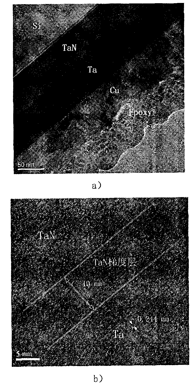
[0032] The present invention adopts self-developed radio frequency reactive magnetron sputtering coating equipment;

[0033] The purity of the sputtering metal Ta target used is 99.99%; the working gases Ar and N 2 The purity is 99.999%;

[0034] The deposition thickness of the double-layer gradient diffusion barrier layer is 100nm;

[0035] The entire deposition process is carried out at room temperature, and this embodiment is a double-layer gradient diffusion barrier layer prepared with optimal process parameters.

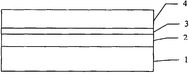
[0036] Under the above conditions, the preparation steps of the Ta / TaN gradient diffusion barrier layer are as follows:

[0037] (1) Treatment of the substrate before deposition

[0038] Put the single crystal Si(111) into acetone for ultrasonic cleaning for 20 minutes, then put it into absolute ethanol for ultrasonic cleaning for 20 minutes, after drying, put it into the vacuum chamber of the radio frequency reaction magnetron sputtering coating equipment, a...

Embodiment 2

[0047] The operation steps of this embodiment, the coating equipment used and other working conditions are all the same as in Example 1, and the total thickness of the double-layer gradient diffusion barrier layer deposition is kept constant at 100nm, and the amorphous TaN layer, TaN gradient layer, and metal TaN layer are adjusted. The deposition time of the layer is changed to change the thickness of each layer of the amorphous TaN layer, the TaN gradient layer and the metal Ta layer in the double-layer gradient diffusion barrier layer.

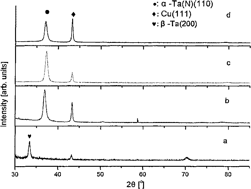
[0048] In this example, the deposition time of the amorphous TaN layer is 3min 50s, and the deposition thickness is 40nm; the deposition time of the TaN gradient layer is 1min, and the deposition thickness is 20nm; the deposition time of the Ta layer is 2min50s, and the deposition thickness is 40nm. / TaN gradient diffusion barrier samples. The obtained samples were analyzed by XRD, and all showed that the generated α-Ta was N solid solution...

Embodiment 3

[0050] The operation steps of this embodiment, the coating equipment used and other working conditions are all the same as in Example 1, and the total thickness of the double-layer gradient diffusion barrier layer deposition is kept constant at 100nm, and the amorphous TaN layer, TaN gradient layer, and metal TaN layer are adjusted. The deposition time of the layer is changed to change the thickness of each layer of the amorphous TaN layer, the TaN gradient layer and the metal Ta layer in the double-layer gradient diffusion barrier layer.

[0051] In this example, the deposition time of the amorphous TaN layer is 3min, and the deposition thickness is 35nm; the deposition time of the TaN gradient layer is 2min20s, and the deposition thickness is 30nm; the deposition time of the Ta layer is 2min20s, and the deposition thickness is 35nm. TaN gradient diffusion barrier layer samples, the obtained samples were analyzed by XRD, all showed that the generated α-Ta was N solid solution,...


PUM

PropertyMeasurementUnit
Deposition thicknessaaaaaaaaaa
Resistivityaaaaaaaaaa
Thicknessaaaaaaaaaa

Abstract

The invention relates to a preparation technique of gradient diffusion impervious layer used for deep submicron integrated circuit Cu interconnection, belonging to the technical field of semiconductor integrated circuit manufacture. In the technique, radio frequency magnetic control sputtering coating equipment is adopted to deposit a layer of amorphous TaN on a monocrystal Si substrate, followed by depositing a TaN gradient layer, the content of N in the gradient coating is adjusted by reducing flow of reactant gas N2 gradually, so that the content of N in the prepared impervious layer decreases progressively from inside to outside; after finishing depositing TaN gradient layer in situ, a metal Ta layer is deposited to obtain the double-layer gradient diffusion impervious layer used for deep submicron integrated circuit Cu interconnection. The resistivity can be as low as 112 mu Omega cm, and the thermostabilization temperature can be over 700 DEG C. The preparation technique has the characteristics of simple operation and convenient promotion; the obtained impervious layer material can improve RC delay of interconnected circuits, and enhance the operation speed and stability of semiconductor elements.

Description

technical field [0001] The invention belongs to the technical field of semiconductor integrated circuit manufacturing technology, and particularly relates to a preparation technology of a low-resistance and high-stability α-Ta / TaN gradient diffusion barrier layer for deep submicron ultra-large-scale integrated circuit Cu interconnection modules. Background technique [0002] With the continuous shrinking of the feature size of integrated circuits and the continuous improvement of integration, Cu has gradually replaced Al as a new generation of interconnection metal materials. However, since Cu can diffuse in Si and Si-based oxide media at low temperature to form deep-level impurities, it has a strong trap effect on the carriers in the device, degrading or even failing the device performance. Therefore, between Cu and Si or SiO 2 A metal barrier layer must be added between them to prevent the diffusion of Cu and improve the bonding performance of Cu and the substrate. In th...

Claims


Application Information

Patent Timeline
IPC IPC(8): H01L21/768
Inventor 刘春海汪渊刘波杨吉军陈顺礼
Owner SICHUAN UNIV
Why Eureka
Try Eureka