Transverse P-type double diffused metal oxide semiconductor transistor of silicon on insulator

An oxide semiconductor and silicon-on-insulator technology, applied in semiconductor devices, electrical components, circuits, etc., can solve the problems of increasing device power consumption, difficult to control, increasing device on-resistance, etc., to achieve process compatibility, prevent punch-through, structure simple effect

Active Publication Date: 2010-05-05
SUZHOU POWERON IC DESIGN
View PDF0 Cites 10 Cited by
  • Summary
  • Abstract
  • Description
  • Claims
  • Application Information

AI Technical Summary

Problems solved by technology

[0005] In related technologies, it has been proposed that the doping concentration of the P-type doped semiconductor region can be reduced, which can not only reduce the peak value of the vertical electric field, improve the vertical withstand voltage value of the device, but also increase the lateral withstand voltage value of the device at the same time, but This approach will greatly increase the on-resistance of the device and increase the power consumption of the device

Method used


Image

  • Transverse P-type double diffused metal oxide semiconductor transistor of silicon on insulator
  • Transverse P-type double diffused metal oxide semiconductor transistor of silicon on insulator
  • Transverse P-type double diffused metal oxide semiconductor transistor of silicon on insulator

Examples


Embodiment Construction

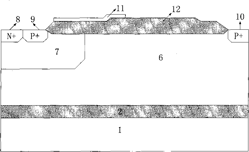
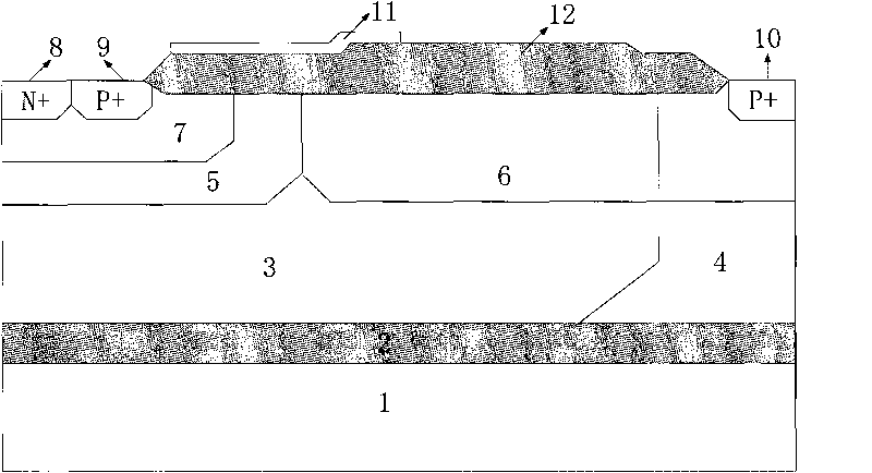
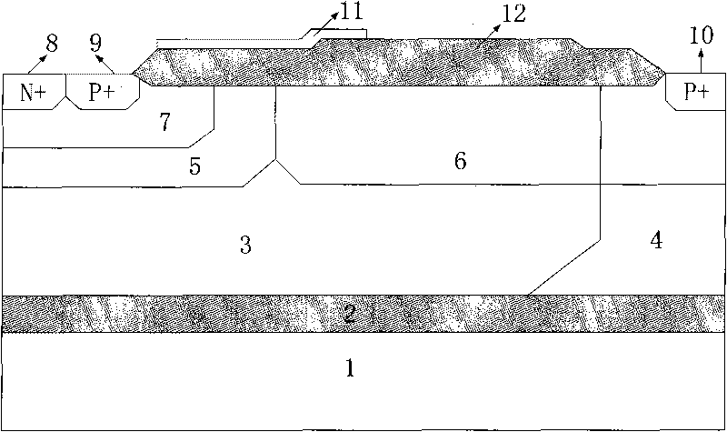
[0017] refer to figure 2 , a silicon-on-insulator lateral P-type double-diffused metal oxide semiconductor transistor, comprising: a semiconductor substrate 1, a buried oxide layer 2 is arranged on the semiconductor substrate 1, and a high-voltage N-type well is arranged on the buried oxide layer 2 3 and a high-voltage P-type well 4, an N-type well 5 and a P-type drift region 6 are arranged on the high-voltage N-type well 3, and the P-type drift region 6 extends to the upper half of the high-voltage P-type well 4, and the N-type well 5 An N-type D well region 7 is arranged on the N-type D well region 7, an N-type contact region 8 and a P-type source region 9 are arranged on the N-type D well region 7, and a drain region 10 is arranged on the P-type drift region 6. In the high-voltage N-type An oxide layer 12 is provided on the surface of the well 3 outside the N-type contact region 8 and the region other than the P-type source region 9 and the region other than the P-type dra...


PUM


Abstract

The invention relates to a transverse P-type double diffused metal oxide semiconductor transistor of silicon on an insulator, which comprises a semiconductor substrate, wherein a buried oxide layer is arranged on the semiconductor substrate, a high-voltage N-type well and a high-voltage P-type well are arranged on the buried oxide layer, an N-type well and a P-type drift region are arranged on the high-voltage N-type well, the P-type drift region extends to the upper half part of the high-voltage N-type well, and an N-type D well region is arranged on the N-type well, thereby forming a three-layered N-type well structure; meanwhile, a step structure exists in an oxide layer on the surface of an element, and the oxide layer on the P-type drift region is obviously thicker than other parts. The transverse P-type double diffused metal oxide semiconductor transistor can effectively improve the pressurization of the element and can prevent puncture between the drift region and a source region.

Description

technical field [0001] The present invention relates to the field of power semiconductor devices, more specifically, it relates to a [0002] Applied silicon-on-insulator lateral P-type double-diffused metal oxide semiconductor transistor (SOI LDMOS) new structure. Background technique [0003] Power semiconductor devices are the basic electronic components for energy control and conversion in power electronic systems. The continuous development of power electronics technology has opened up a wide range of application fields for semiconductor power devices, and the characteristics of semiconductor power devices such as on-resistance and breakdown voltage determine The basic performance of the power electronic system, such as efficiency and power consumption. Modern power electronic devices and related products represented by lateral double-diffused metal-oxide-semiconductor transistors are playing an increasingly important role in industries, energy, transportation, and oth...

Claims


Application Information

Patent Timeline
IPC IPC(8): H01L29/78H01L29/06H01L29/36
CPCH01L29/7824
Inventor 易扬波王钦刘侠李海松陈文高
Owner SUZHOU POWERON IC DESIGN
Why Eureka
Try Eureka