Method for manufacturing semiconductor chip with low warpage

A semiconductor, low warpage technology, used in semiconductor/solid-state device manufacturing, electrical components, circuits, etc., can solve the problems of increasing the warpage of semiconductor wafers, increasing the cracking of semiconductor wafers, reducing product performance and yield, etc. Effects of increased ductility, reduced stress, low warpage

Active Publication Date: 2010-06-09
SEMICON MFG INT (SHANGHAI) CORP
View PDF0 Cites 6 Cited by
  • Summary
  • Abstract
  • Description
  • Claims
  • Application Information

AI Technical Summary

Problems solved by technology

For example: the intermetal dielectric layer or metal interconnection layer in the layer structure of the semiconductor wafer will increase the stress of the layer structure itself or the interlayer structure due to its own material characteristics, or the semiconductor film will also cause the temperature and humidity changes in the external environment. Changes in stress, which will increase the warpage of the semiconductor wafer, increase the probability of semiconductor wafer cracking, and reduce the performance and yield of the product

Method used


Image

  • Method for manufacturing semiconductor chip with low warpage
  • Method for manufacturing semiconductor chip with low warpage
  • Method for manufacturing semiconductor chip with low warpage

Examples


Embodiment Construction

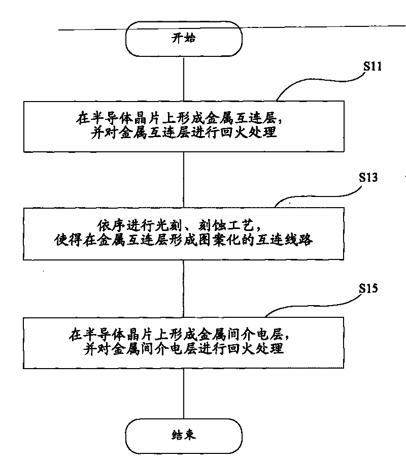
[0025] The embodiment of the present invention preliminarily provides a semiconductor carrier wafer with low warpage. On this basis, at least one tempering step is included in the process of the intermetal dielectric layer and the metal interconnection layer, and the intermetal dielectric layer is fabricated. The oxygen-enriched silicon dioxide deposition process and the FGS deposition process further include controlling the waiting time to reduce the stress of the intermetallic dielectric layer, metal interconnection layer, and semiconductor film in the semiconductor wafer, so that the semiconductor wafer can obtain low The effect of warpage.

[0026] In order to make the above objects, features and advantages of the present invention more comprehensible, specific implementations of the present invention will be described in detail below in conjunction with the accompanying drawings.

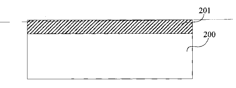
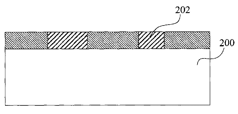
[0027] The manufacturing method of the semiconductor wafer in the embodiment of the present...


PUM


Abstract

The invention discloses a method for manufacturing a semiconductor chip with low warpage. The semiconductor chip is provided with a semiconductor device; a process for manufacturing an inter-metal dielectric layer and a metal interconnecting layer comprises at least once tempering step, so the movability of atoms of the inter-metal dielectric layer and the metal interconnecting layer is improved, the tractility of the two is increased, the stress of the two is correspondingly reduced, and the semiconductor chip has the advantage of low warpage.

Description

technical field [0001] The invention relates to a method for manufacturing a semiconductor wafer with low warpage. Background technique [0002] The deformation of the semiconductor wafer will occur during the manufacturing process and later when the circuit and electronic components are made on the semiconductor wafer. Deformation will affect the quality of the semiconductor wafer. For example, during the photolithography process, if the semiconductor wafer is deformed, the illuminated surface will be uneven. In this case, the mask structure in all regions of the semiconductor wafer cannot form a clear image. In addition, the mask structure transferred to the semiconductor wafer will move sideways, resulting in overlap of adjacent components, which cannot perform its function. [0003] Generally, "warpage" can be used to describe the overall shape of a semiconductor wafer. Warpage refers to the maximum deviation of any two points on the middle surface of the semiconductor...

Claims


Application Information

Patent Timeline
Patent Type & Authority Applications(China)
IPC IPC(8): H01L21/768
Inventor 李景伦赵洪波华宇郑召星
Owner SEMICON MFG INT (SHANGHAI) CORP
Why Eureka
Try Eureka