Preparation method of crystal silicon solar cell
A technology of solar cells and crystalline silicon, applied in the field of solar photovoltaic utilization, can solve the problems of expensive, unsuitable for large-scale, and low-cost industrial production, and achieve the effects of easy operation, good application prospects, and improved conversion efficiency
- Summary
- Abstract
- Description
- Claims
- Application Information
AI Technical Summary
Problems solved by technology
Method used
Image
Examples
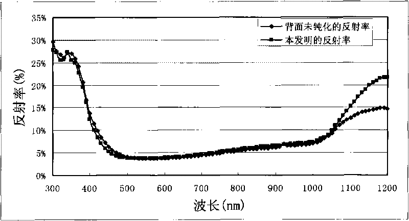
Embodiment 1
[0023] See attached figure 1 Shown, a kind of preparation method of crystalline silicon solar cell comprises the steps:
[0024] (1) Clean the silicon wafer and make the surface texture;
[0025] (2) Perform phosphorus diffusion to form a PN junction;
[0026] (3) Etching, dephosphorous silicon glass cleaning;
[0027] (4) Form a passivation layer on the front surface by PECVD or magnetron sputtering;
[0028] (5) A single-layer passivation layer is formed on the back surface by thermal oxidation, and the structure of the passivation layer is SiO 2 (The passivation layer can also be a-Si, SiC, SiNx, etc.), with a thickness of 20nm;
[0029] (6) Utilize the method of ink-jet printing corrosive paste, open contact window on the back passivation layer, the technological process of opening contact window on the surface of solar cell back passivation layer is: adopt the method for ink-jet printing to passivate on the back side Print corrosive slurry on the layer, the wet weigh...
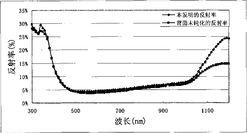
Embodiment 2
[0035] See attached figure 2 Shown, a kind of preparation method of crystalline silicon solar cell comprises the steps:
[0036] (1) Clean the silicon wafer and make the surface texture;
[0037] (2) Perform phosphorus diffusion to form a PN junction;
[0038] (3) Etching, dephosphorous silicon glass cleaning;
[0039] (4) Form a passivation layer on the front surface by PECVD or magnetron sputtering;
[0040] (5) A single-layer passivation layer is formed on the back surface by PECVD, and the structure of the passivation layer is SiO 2 (The passivation layer can also be a-Si, SiC, SiNx, etc.), with a thickness of 50nm;
[0041] (6) Utilize the method of ink-jet printing corrosive paste, open contact window on the back passivation layer, the technological process of opening contact window on the surface of solar cell back passivation layer is: adopt the method for ink-jet printing to passivate on the back side Print corrosive slurry on the layer, the wet weight of corros...
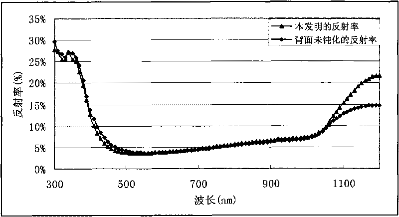
Embodiment 3
[0047] See attached image 3 Shown, a kind of preparation method of crystalline silicon solar cell comprises the steps:
[0048] (1) Clean the silicon wafer and make the surface texture;
[0049] (2) Perform phosphorus diffusion to form a PN junction;
[0050] (3) Etching, dephosphorous silicon glass cleaning;
[0051] (4) Form a passivation layer on the front surface by PECVD or magnetron sputtering;
[0052] (5) Utilize the PECVD method to form a single-layer passivation layer on the back surface, the structure of the passivation layer is SiNx (the passivation layer can also be a-Si, SiC, SiO 2 etc.), the thickness is 60nm;
[0053] (6) Utilize the method of ink-jet printing corrosive paste, open contact window on the back passivation layer, the technological process of opening contact window on the surface of solar cell back passivation layer is: adopt the method for ink-jet printing to passivate on the back side Print corrosive slurry on the layer, the wet weight of c...
PUM
| Property | Measurement | Unit |
|---|---|---|
| Thickness | aaaaa | aaaaa |
| Thickness | aaaaa | aaaaa |
Abstract
Description
Claims
Application Information


