

Method for preparing material with highly gradient surface micronano structure
A technology of micro-nano structure and target materials, applied in the field of nano-material processing, to achieve the effects of rapid construction, breakthrough of space limitations, and simple operation
Inactive Publication Date: 2010-06-16
PEKING UNIV
View PDF3 Cites 2 Cited by
- Summary
- Abstract
- Description
- Claims
- Application Information
AI Technical Summary
Problems solved by technology
However, these methods are difficult to construct an ideal structure with a high degree of gradient and a smooth surface.
Method used
View moreImage
Smart ImageViewing Examples

Examples
Embodiment 1
Embodiment 2
Embodiment 3
Login to View More PUM
 Abstract
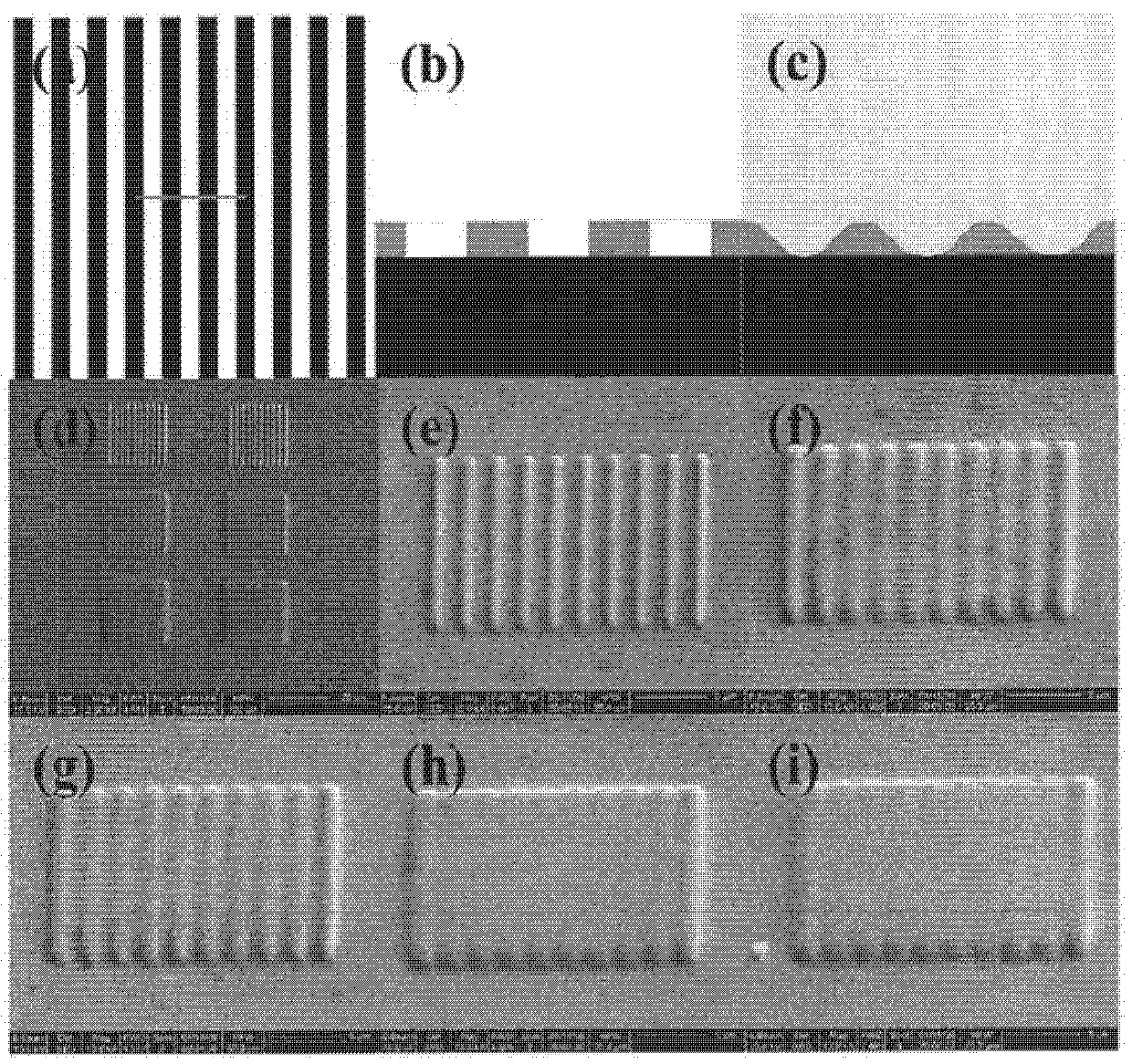
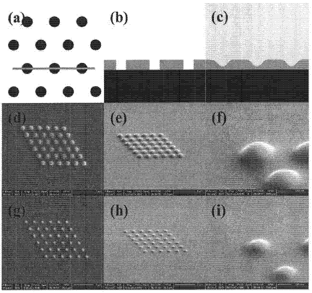
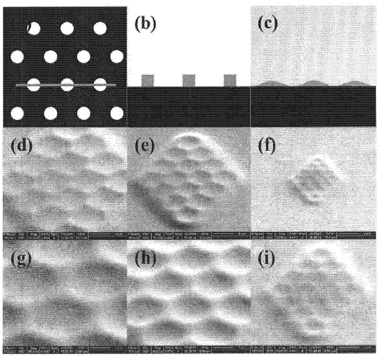
The invention discloses a method for preparing a material with a highly gradient surface micronano structure. The method comprises the following steps of: 1) coating an electron beam resist on a substrate to obtain an electron beam resist layer, and baking the electron beam resist layer ; 2) exposing, developing and fixing electron beams; 3) coating anisole to obtain an anisole layer, and baking the anisole layer; 4) depositing a target material on the anisole layer to obtain a target material layer; 5) attaching the target material layer to another substrate; and 6) separating the target material layer from the electron beam resist layer. The method has the advantages of simple and convenient operation mode, wide material application range, customized shape and position of a pattern, smooth structural surface and high controllability and repeatability, and can play an important role in fields of surface plasmon research, self assembly of nano particles, utilization of solar energy, micro-flow research and the like.
Description
technical field The invention relates to the field of nanomaterial processing, and relates to a method for preparing a material with a micro-nano structure, in particular to a method for preparing a material with a surface micro-nano structure. Background technique The structure of surface micro- and nanostructures is of great significance in many fields, and has played a huge role in surface plasmons, self-assembly of nanoparticles, solar energy utilization, and microfluidic devices (H. Ditlbacher, J.R. Krenn, G. Schider et al. Applied Physics Letters, 81, 1762 (2002); M.J. Lee, J. Kim and Y.S. Nanotechnology, 19, 355301 (2008); A. Lasagni, M. Nejati, R. Clasen et al. Advanced Functional Materials, 8, 580 (2006); S. Billat, K. Kliche, R. Gronmaier et al. Sensors and Actuators A: Physical, 145-146, 66 (2008)). Along with the trend of device miniaturization, various micro-nano-fabrication methods have been greatly developed, so as to obtain simple and precise control of the ...
Claims
Login to View More Application Information
Patent Timeline
 Patent Type & AuthorityApplications(China)
IPC IPC(8): B82B3/00
Inventor张洋朱新利俞大鹏
OwnerPEKING UNIV