Method for preparing CdS film used for window layer of solar battery
A solar cell and window layer technology, which is applied in the manufacture of circuits, electrical components, and final products. It can solve the problems of CdS thin films that cannot be deposited, that the films are not strong enough, and that the films are not uniform enough, so as to reduce the impurity concentration, prevent falling off, and reduce mutual The effect of diffusion
- Summary
- Abstract
- Description
- Claims
- Application Information
AI Technical Summary
Problems solved by technology
Method used
Image
Examples
Embodiment 1
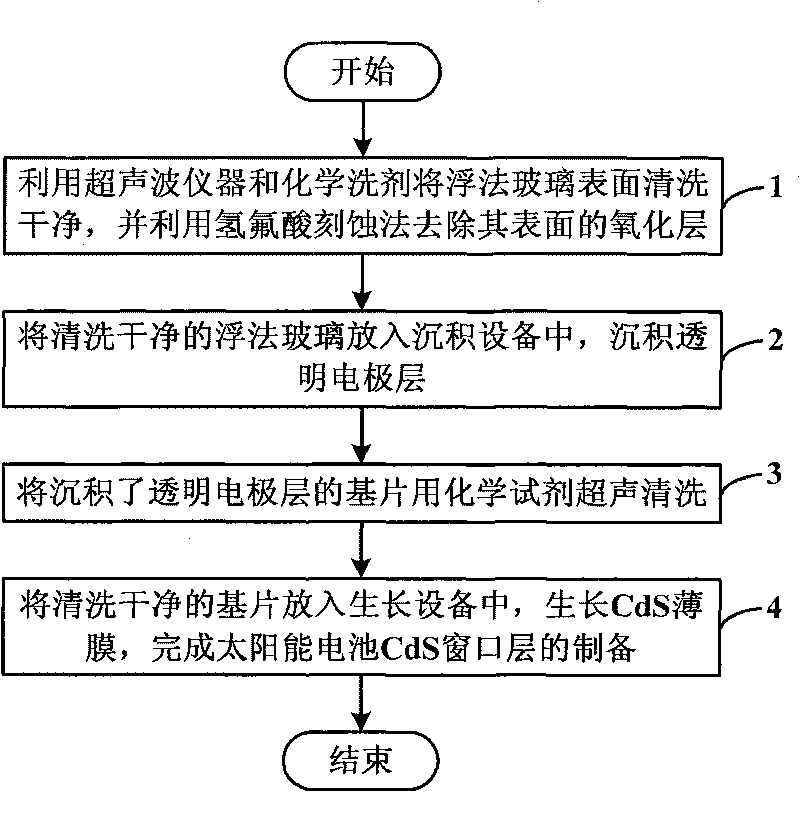
[0040] The specific steps of growing a CdS film after depositing a transparent electrode ITO on a glass substrate are as follows (in conjunction with referring to figure 2 ):
[0041] After immersing the glass substrate in chemical detergent, clean the surface of the substrate with an ultrasonic cleaning device, and remove inorganic substances and oxides on the surface with nitric acid, sulfuric acid, hydrogen peroxide and hydrochloric acid;
[0042] Slowly place the cleaned glass substrate on the substrate stage of the magnetron sputtering equipment and fix it, and grow a 500nm ITO transparent electrode layer. During sputtering, the substrate temperature is 300°C and the gas pressure is 3×10 -3 Pa;
[0043] After the deposited ITO substrate was ultrasonically cleaned with a chemical detergent, it was slowly placed on the substrate stage of the sputtering equipment, fixed and stable, and then the CdS film was grown. The magnetron sputtering equipment for growth includes ra...
Embodiment 2
[0048] Deposition of transparent electrode SnO on glass substrate 2 : The specific steps of growing CdS film after F are as follows (in conjunction with reference figure 2 ):
[0049] After immersing the glass substrate in chemical detergent, clean the surface of the substrate with an ultrasonic cleaning device, and remove inorganic substances and oxides on the surface with nitric acid, sulfuric acid, hydrogen peroxide and hydrochloric acid;
[0050] Slowly put the cleaned glass substrate into the CVD equipment and fix it, grow a layer of 500nm SnO 2 : F transparent electrode layer.
[0051] Will deposit good SnO 2 After the substrate of :F is ultrasonically cleaned with a chemical lotion, it is slowly placed on the substrate stage of the sputtering equipment, and then the CdS thin film is grown after being fixed and stable. The magnetron sputtering equipment for growth includes radio frequency power supply, reaction chamber, rotatable substrate stage, target stage for pl...
Embodiment 3
[0056] The specific steps of growing a CdS film after depositing a transparent electrode ITO on a glass substrate are as follows (in conjunction with referring to figure 2 ):
[0057] After immersing the glass substrate in chemical detergent, clean the surface of the substrate with an ultrasonic cleaning device, and remove inorganic substances and oxides on the surface with nitric acid, sulfuric acid, hydrogen peroxide and hydrochloric acid;
[0058] Slowly place the cleaned glass substrate on the substrate stage of the magnetron sputtering equipment and fix it, and grow a 400nm ITO transparent electrode layer. During sputtering, the substrate temperature is 400°C and the gas pressure is 3×10 -3 Pa;
[0059] After the deposited ITO substrate was ultrasonically cleaned with a chemical detergent, it was slowly placed on the substrate stage of the sputtering equipment, fixed and stable, and then the CdS film was grown. The magnetron sputtering equipment for growth includes ra...
PUM
 Abstract
Description
Claims
Application Information


