Electrical inductance in integrated circuit and manufacturing method

A technology of integrated circuits and manufacturing methods, which is applied in the manufacture of circuits, electrical components, semiconductors/solid-state devices, etc., and can solve problems such as limited magnetic field strength

Inactive Publication Date: 2010-06-23
SHANGHAI HUA HONG NEC ELECTRONICS
View PDF0 Cites 11 Cited by
  • Summary
  • Abstract
  • Description
  • Claims
  • Application Information

AI Technical Summary

Problems solved by technology

But the inductance that adopts prior art method to make is only on single-layer metal, and doe

Method used


Image

  • Electrical inductance in integrated circuit and manufacturing method
  • Electrical inductance in integrated circuit and manufacturing method
  • Electrical inductance in integrated circuit and manufacturing method

Examples


Embodiment Construction

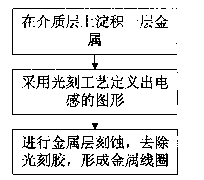
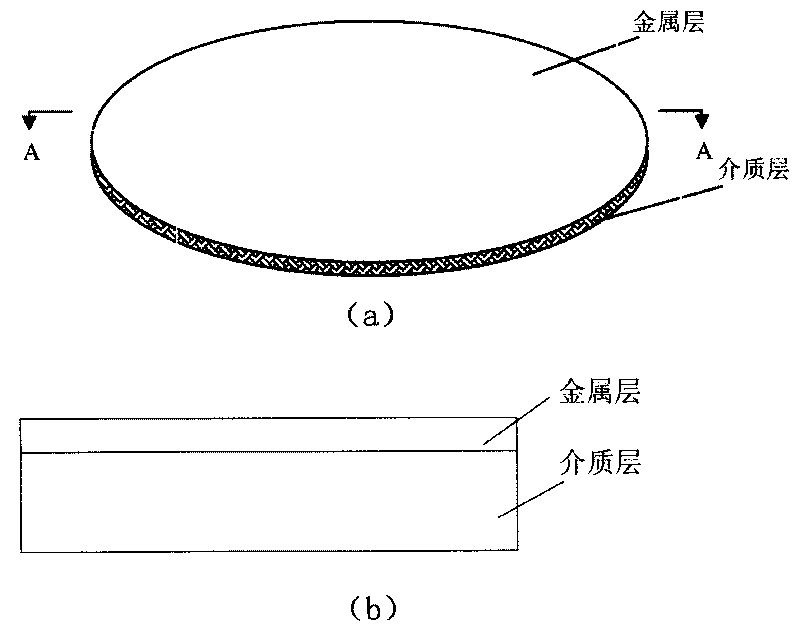
[0031] Such as Figure 6 As shown, the manufacturing method of the inductance in the integrated circuit of the present invention, the whole process all is to finish on silicon substrate, and silicon substrate is not reflected in accompanying drawing, and the present invention comprises the following steps:

[0032] first step, such as Figure 7 As shown, a layer of metal is deposited on the dielectric layer, generally metal aluminum is used, of course, a metal barrier layer is formed by sputtering before depositing the metal layer.

[0033] The second step, such as Figure 8 As shown, the pattern of the inductor is defined by the photolithography process. That is, apply photoresist on the entire metal layer, and then use a photolithographic mask to perform photolithography. You can use positive photoresist or negative photoresist, and finally develop to form the required inductance. graphics. The inductance pattern here is determined by the layout, and can be a ring formed...


PUM


Abstract

The invention discloses an electrical inductance in an integrated circuit and a manufacturing method, comprising the following steps: 1, a metal layer is deposited on a dielectric layer; 2, the diagram of the electrical inductance is defined through adopting photoetching technology; 3, the etching is conducted on the metal layer, and the optical resist is removed, and a metal coil is formed; 4, the dielectric layer continues to be deposited, and a through hole is formed at the dielectric layer; 5, the filling metal is filled in the through hole; 6, step 1-step 5 are repeated to increase the number of layers of the electrical inductance, until the last layer of metal coil is formed. The electrical inductance in the integrated circuit contains a plurality of layers of metal coils in parallel, and the adjacent metal coils are connected through connecting contact holes. The electrical inductance of the integrated circuit which is manufactured through utilizing the manufacturing method of the invention comprises the plurality of metal coils, and increases the magnetic-field strength of the electrical inductance.

Description

technical field [0001] The invention relates to an integrated circuit manufacturing process, in particular to an inductor in an integrated circuit and a method for manufacturing the inductor. Background technique [0002] At present, the manufacturing method of inductors in integrated circuits is generally to use a certain metal layer to manufacture inductors formed by multiple turns of metal wires on a single layer. The layout of commonly used metal inductors is as follows figure 1 shown. [0003] In the prior art, one inductor can be prepared in a single layer, and multiple inductors can also be prepared. Now, two inductors are prepared in a single layer as an example to illustrate the method of manufacturing inductors in the prior art. The steps are as follows figure 2 As shown, the following steps are included: the first step, such as image 3 As shown in a, a layer of metal is deposited on the dielectric layer, usually metal aluminum, along the image 3 The profile...

Claims


Application Information

Patent Timeline
IPC IPC(8): H01L21/02H01L21/768H01L21/82
Inventor 陈华伦罗啸熊涛陈瑜陈雄斌
Owner SHANGHAI HUA HONG NEC ELECTRONICS
Why Eureka
Try Eureka