TFT-LCD (Thin Film Transistor Liquid Crystal Display) array base plate and drive method thereof

A technology of array substrates and substrates, applied in optics, instruments, electrical components, etc., can solve problems such as the reduction of the aperture ratio of the pixel area and the influence of data lines on the display performance, so as to reduce the number of scan driver chips or the number of scan driver chip pins, The effect of reducing the number of gate lines and the number of scanning driver chips or the number of pins of scanning driver chips, and reducing production costs

Active Publication Date: 2010-06-30
BOE TECH GRP CO LTD +1
View PDF0 Cites 38 Cited by
  • Summary
  • Abstract
  • Description
  • Claims
  • Application Information

AI Technical Summary

Problems solved by technology

Increasing the number of data lines, if the length of the data lines is too long will cause display problems such as signal delay; if the line width of the data lines is increased in order to reduce the signal delay, the aperture ratio of the pixel area will decrease, and at the edge of the data lines Also prone to defects that affect display performance

Method used


Image

  • TFT-LCD (Thin Film Transistor Liquid Crystal Display) array base plate and drive method thereof
  • TFT-LCD (Thin Film Transistor Liquid Crystal Display) array base plate and drive method thereof
  • TFT-LCD (Thin Film Transistor Liquid Crystal Display) array base plate and drive method thereof

Examples


Embodiment Construction

[0042] The technical solutions of the present invention will be described in further detail below with reference to the accompanying drawings and embodiments.

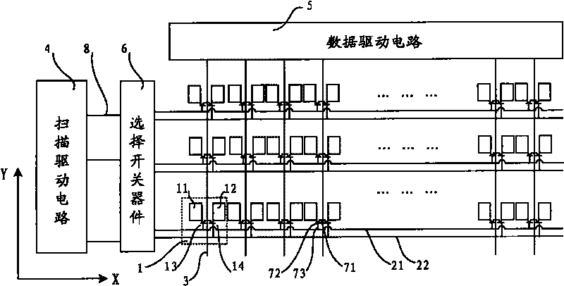
[0043] figure 1 It is a structural schematic diagram of the first embodiment of the TFT-LCD array substrate of the present invention. Such as figure 1 As shown, the TFT-LCD array substrate of the present invention includes a substrate, a display area formed on the substrate and a peripheral area other than the display area, and the display area is composed of pixel areas arranged in a matrix. Two pixel electrodes and two thin film transistors are formed in each pixel area; figure 1 The X direction shown in ) is provided with a selection switch device 6 on the peripheral area, and the gate line is connected with the scanning drive circuit 4 through the selection switch device 6; along the extending direction of the data line 3 (that is, along the figure 1A data drive circuit 5 is connected to the peripheral area in t...


PUM


Abstract

The invention relates to a TFT-LCD array base plate and a drive method thereof. The array base plate comprises a base plate, wherein the base pate is provided with pixel areas which are ranged in a matrix way; each pixel area is provided with a first pixel electrode, a first film transistor, a second pixel electrode and a second film transistor, the first pixel electrode and the first film transistor are positioned in an odd line, and the second pixel electrode and the second film transistor are positioned in an even line; a first grid line and a second grid line are arranged in each pixel area, the first grid line is connected with a grid electrode of the first film transistor, and the second grid line is connected with a grid electrode of the second film transistor; and a data line is arranged in each pixel area and respectively connected with a source electrode of the first film transistor and a source electrode of the second film transistor. The invention reduces the quantity of the data lines and data drive chips or pins thereof or reduces the quantity of the grid lines and scanning drive chips or pins thereof and lowers the production cost of a TFT-LCD.

Description

technical field [0001] The invention relates to a liquid crystal display device and a driving method thereof, in particular to a TFT-LCD array substrate and a driving method thereof. Background technique [0002] Thin Film Transistor Liquid Crystal Display (TFT-LCD for short) mainly includes: a liquid crystal display panel, a scanning drive circuit and a data drive circuit; wherein, the liquid crystal display panel includes a color film substrate and an array substrate arranged in a box, and a set The liquid crystal layer between the two substrates; the scan driving circuit and the data driving circuit are respectively connected with the TFT switching elements on the array substrate. [0003] In a traditional TFT-LCD array substrate, a TFT switch element is controlled by a data line (DataLine) and a gate line (Gate Line), and the pixel electrode connected to the TFT switch element is driven by turning on or off the TFT switch element. When the array substrate is working, th...

Claims


Application Information

Patent Timeline
Patent Type & Authority Applications(China)
IPC IPC(8): G02F1/1362H01L27/12G09G3/36
CPCG09G3/3648G02F1/136286G09G2310/02G09G2300/0426
Inventor 马占洁
Owner BOE TECH GRP CO LTD
Why Eureka
Try Eureka