Method for producing nano graphite field emission vacuum electronic cathode

A technology of nano-graphite and vacuum electronics, applied in cold cathode manufacturing, electrode system manufacturing, discharge tube/lamp manufacturing, etc., can solve the problems of complex production process, large volume, low production efficiency, etc., and achieve easy industrial production and production The effect of simple process and high production efficiency

Inactive Publication Date: 2010-06-30
UNIV OF ELECTRONICS SCI & TECH OF CHINA
View PDF0 Cites 8 Cited by
  • Summary
  • Abstract
  • Description
  • Claims
  • Application Information

AI Technical Summary

Problems solved by technology

[0002] The cathode of traditional microwave vacuum electronic devices is generally made of tungsten oxide or tungsten related materials, which belongs to hot cathode emission; the electron emission cathode used in traditional projection tube electronic devices also relies on thermionic emission, so the existence efficiency is low and the working temperature is low. High and preheating, as well as large volume, high power consumption and other defects; for these defects and the use of nano-graphite as a field emission cathode technology is the use of chemical vapor deposition growth, or the method of making a film after dispersion with a solvent to obtain nano Graphite film, and then made into a planar film-shaped field emission electron cathode, that is, a cathode that emits electrons through the graphite film plane; although this type of electron cathode has the advantages of high emission efficiency and high current density, it is generally only used in cold In terms of cathode field emission flat panel display, it is difficult to be used in tube-type vacuum electronic devices such as field emission microwave tubes, digital tubes, and projection tubes, and there are disadvantages such as complex production processes, low production efficiency, and high production costs.

Method used


Image

  • Method for producing nano graphite field emission vacuum electronic cathode
  • Method for producing nano graphite field emission vacuum electronic cathode
  • Method for producing nano graphite field emission vacuum electronic cathode

Examples


Embodiment Construction

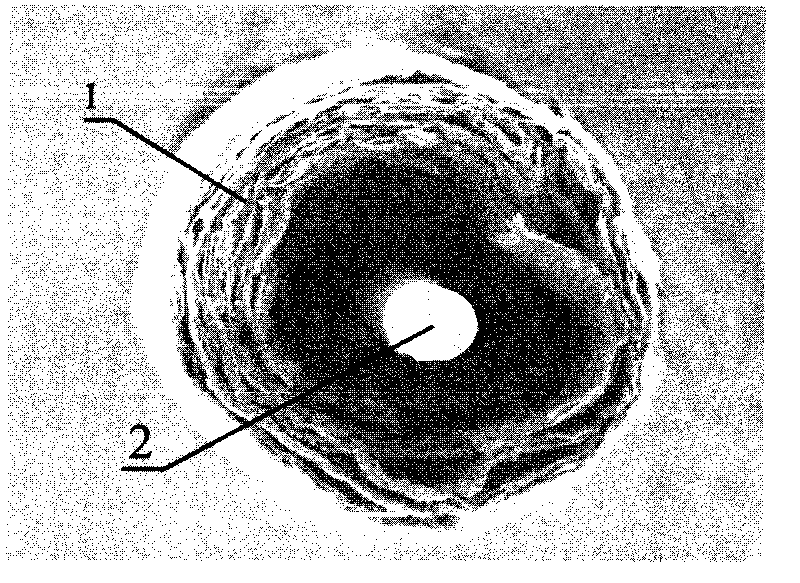
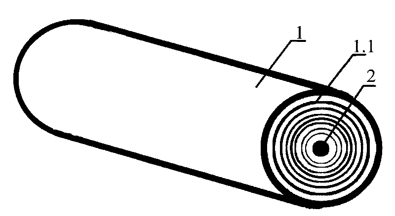
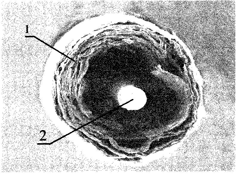
[0016] A. Put 4.0g of industrial expanded graphite with a thickness of 0.1-100μm into a high-temperature-resistant container, heat it at 800±20°C to fully expand it, and obtain worm-like expanded graphite;

[0017] B. be after the industrial concentrated sulfuric acid 500ml of 96% and 1.0g potassium permanganate are mixed with solution with concentration, add step A gained expanded graphite, oxidize to thickness≤1nm, side length is the nano-graphite sheet (sheet) of 1-10 μm shape particles), the resulting mixed solution containing nano-graphite flakes is transferred to step C;

[0018] C. After filtering the mixed solution obtained in step B, washing with water to remove acid, then placing it in deionized water, performing ultrasonic and centrifugal purification treatment under the condition of ultrasonic frequency of 100KHz and power of 50W, and collecting the upper layer after the impurities are separated at the bottom Liquid, obtain the suspension of dispersed oxidized grap...


PUM

PropertyMeasurementUnit
thicknessaaaaaaaaaa
lengthaaaaaaaaaa
thicknessaaaaaaaaaa

Abstract

The invention belongs to the field of vacuum electronic element and device production and a method for producing field emission microwave vacuum electronic cathode by using a nano graphite material. The method comprises: processing industrial expanded graphite sheets at high temperature to produce wormlike expanded graphite; processing the wormlike expanded graphite with solution of concentrated sulfuric acid and potassium permanganate to produce nano graphite sheets; washing the nano graphite sheets to remove acid and purifying the nano graphite sheets by using ultrasonic waves and centrifugation; filtering and drying the nano graphite sheets and forming a film; rolling up the film to produce a nano graphite cylinder; and subjecting the nano graphite column to calcining and post treatment to obtain the nano graphite cylindrical cathode. The method has the characteristics that: the production process is simple, reliable, low in energy consumption and high in production efficiency; the produced electronic cathode has a small cross section and high stability, can emit high-intensity current in use, makes the industrial production realized easily; and the like. The method overcome the drawbacks of the prior art such as difficult use in field emission microwave tubes, digital tubes, projection tubes and other tube vacuum electronic elements, complicated production process, low production efficiency, high production cost and the like.

Description

technical field [0001] The invention belongs to the field of vacuum electronic components and device production, in particular to a production method of a field emission microwave vacuum electron cathode produced by nano-graphite materials. , Nixie tubes, projection tubes and other tube-type vacuum electronic devices for the cathode. Background technique [0002] The cathode of traditional microwave vacuum electronic devices is generally made of tungsten oxide or tungsten related materials, which belongs to hot cathode emission; the electron emission cathode used in traditional projection tube electronic devices also relies on thermionic emission, so the existence efficiency is low and the working temperature is low. High and preheating, as well as large volume, high power consumption and other defects; for these defects and the use of nano-graphite as a field emission cathode technology is the use of chemical vapor deposition growth, or the method of making a film after dis...

Claims


Application Information

Patent Timeline
Patent Type & Authority Applications(China)
IPC IPC(8): H01J9/02
Inventor 曾葆青柳建龙吴喆刘兴翀
Owner UNIV OF ELECTRONICS SCI & TECH OF CHINA
Why Eureka
Try Eureka