

Conducting structure for semiconductor integrated circuit and forming method thereof
A conductive structure and integrated circuit technology, which is applied in the direction of semiconductor devices, semiconductor/solid-state device manufacturing, semiconductor/solid-state device components, etc. sexual connection
- Summary
- Abstract
- Description
- Claims
- Application Information
AI Technical Summary
Problems solved by technology
Method used
Image

Examples
Embodiment Construction
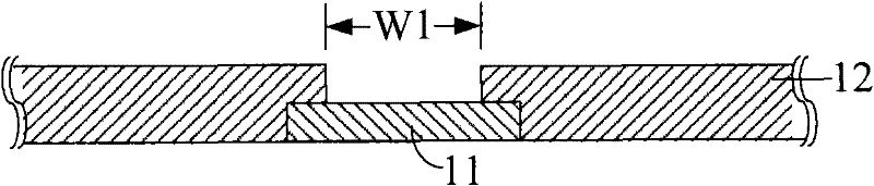
[0013] Figure 1(a) to Figure 1(h) A preferred embodiment of the present invention is shown, which is a schematic flow chart of the formation of a conductive structure for a semiconductor integrated circuit.
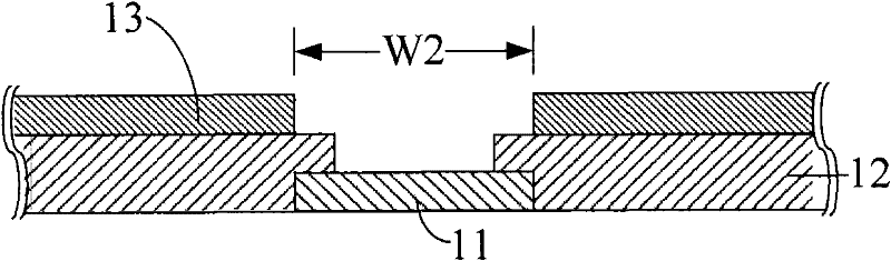
[0014] FIG. 1( a ) shows the initial manufacturing process, which firstly forms a liner 11 and a protective layer 12 . In this embodiment, the liner 11 is made of aluminum, and the protective layer 12 partially covers the liner 11, so that the liner 11 is exposed to define a first opening area, which is used as an electrical contact with a bump later. The connection window, wherein the first opening area has a first lateral dimension W1. Since the protective layer 12 covers the edge of the pad 11, the first opening area is smaller than the lateral dimension of the pad.
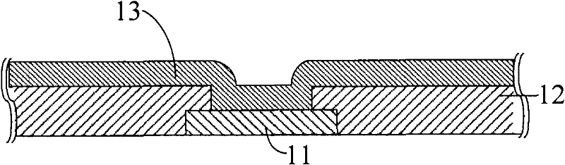
[0015] Then form a first conductive layer, such as a titanium-tungsten alloy conductive layer 13, which covers the first opening area and extends on the protective layer 12 when it is formed; as shown i...
PUM
 Abstract
Description
Claims
Application Information