Flash memory structure
A flash memory and nitride technology, used in electrical components, electrical solid devices, circuits, etc., can solve the problems of reduced thickness of the dielectric structure, easy charge escape, and difficult to control the thickness, so as to improve the retention capacity and overcome the change of the dielectric structure. Thin, loss-free effect
- Summary
- Abstract
- Description
- Claims
- Application Information
AI Technical Summary
Problems solved by technology
Method used
Image

Examples
Embodiment Construction
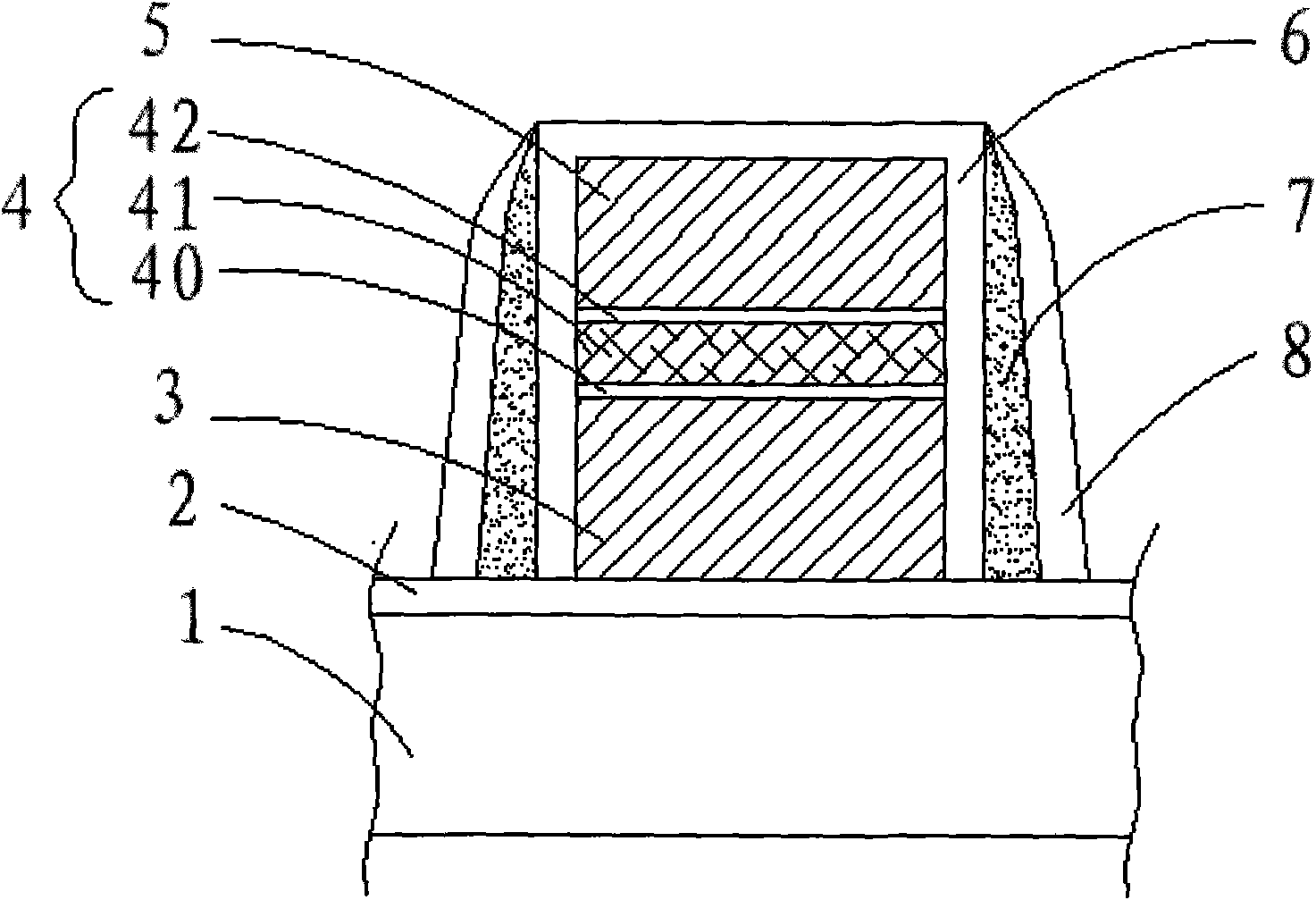
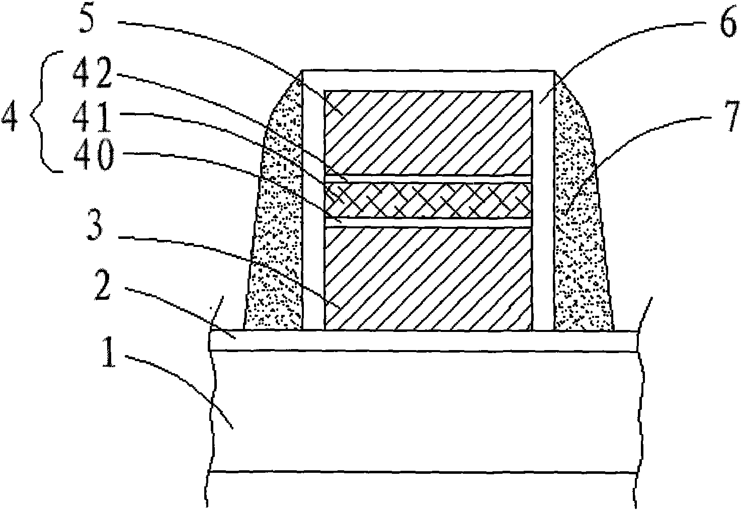
[0027] For the flash memory structure provided in this embodiment, please refer to figure 2 , the flash memory structure includes: a semiconductor substrate 1, which is provided with multiple ion-doped regions to serve as source (not marked) and drain (not marked) respectively, and a layer of tunnel oxide layer is formed on the surface of the substrate 1 2. A floating gate 3 is arranged above the tunnel oxide layer 2, the floating gate 3 is located between the source and the drain, and an insulating layer 4 is connected to the upper surface of the floating gate 3, and the insulating layer 4 can be The composition of oxide and nitride, oxide or nitride, such as the dielectric structure of ONO (oxide-nitride-oxide) or the dielectric structure of ON (oxide-nitride), in this embodiment, the The insulating layer 4 is a dielectric structure in which silicon oxide 40 , silicon nitride 41 and silicon oxide 42 are stacked. A control gate 5 is stacked over the insulating layer 4 . Th...
PUM
| Property | Measurement | Unit |
|---|---|---|
| Thickness | aaaaa | aaaaa |
| Thickness | aaaaa | aaaaa |
| Thickness | aaaaa | aaaaa |
Abstract
Description
Claims
Application Information