Full transparent AlGaN/GaN high electron mobility transistor and manufacturing method thereof

A technology with high electron mobility and fabrication method, applied in semiconductor/solid-state device manufacturing, circuits, electrical components, etc., can solve the problem that the breakdown field strength and material mobility are not as good as GaN materials, limit the application of AlGaN/GaN HEMT, and cannot achieve full Transparent electronic device application and other issues, to achieve the effect of improving electrical conductivity and improving anti-radiation characteristics

Active Publication Date: 2010-07-07
云南凝慧电子科技有限公司
View PDF0 Cites 19 Cited by
  • Summary
  • Abstract
  • Description
  • Claims
  • Application Information

AI Technical Summary

Problems solved by technology

However, the gate, source, and drain contacts of AlGaN / GaN HEMTs with conventional structures are opaque metal materials, which limits the application of AlGaN / GaN HEMTs in the field of transparent electronic devices.
The AlGaN / GaNHEMT that uses ITO material to make the gate only realizes the transparency of the gate electrode, but the source and drain electrodes do not use transparent materials, so it cannot realize the application of fully transparent electronic devices
Although ZnO-based transparent transistors can be used in transparent fields, because the breakdown field strength and material mobility of ZnO materials are not as good as those of GaN materials, there are still many shortcomings in the application of ZnO-based transistors in the field of high-performance transparent electronic devices.

Method used


Image

  • Full transparent AlGaN/GaN high electron mobility transistor and manufacturing method thereof
  • Full transparent AlGaN/GaN high electron mobility transistor and manufacturing method thereof
  • Full transparent AlGaN/GaN high electron mobility transistor and manufacturing method thereof

Examples


Embodiment 1

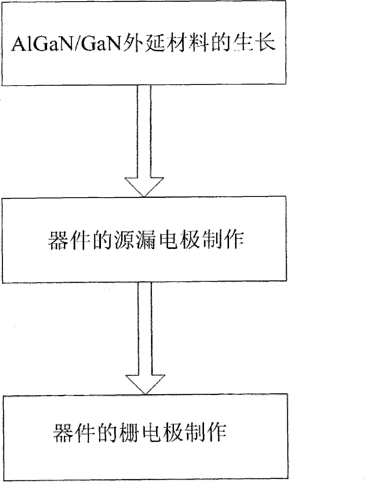
[0031] Embodiment 1, the making of device of the present invention, comprises the following steps:

[0032] Step 1. Epitaxial material growth.

[0033] refer to figure 1 and figure 2 , the specific implementation of this step is as follows:

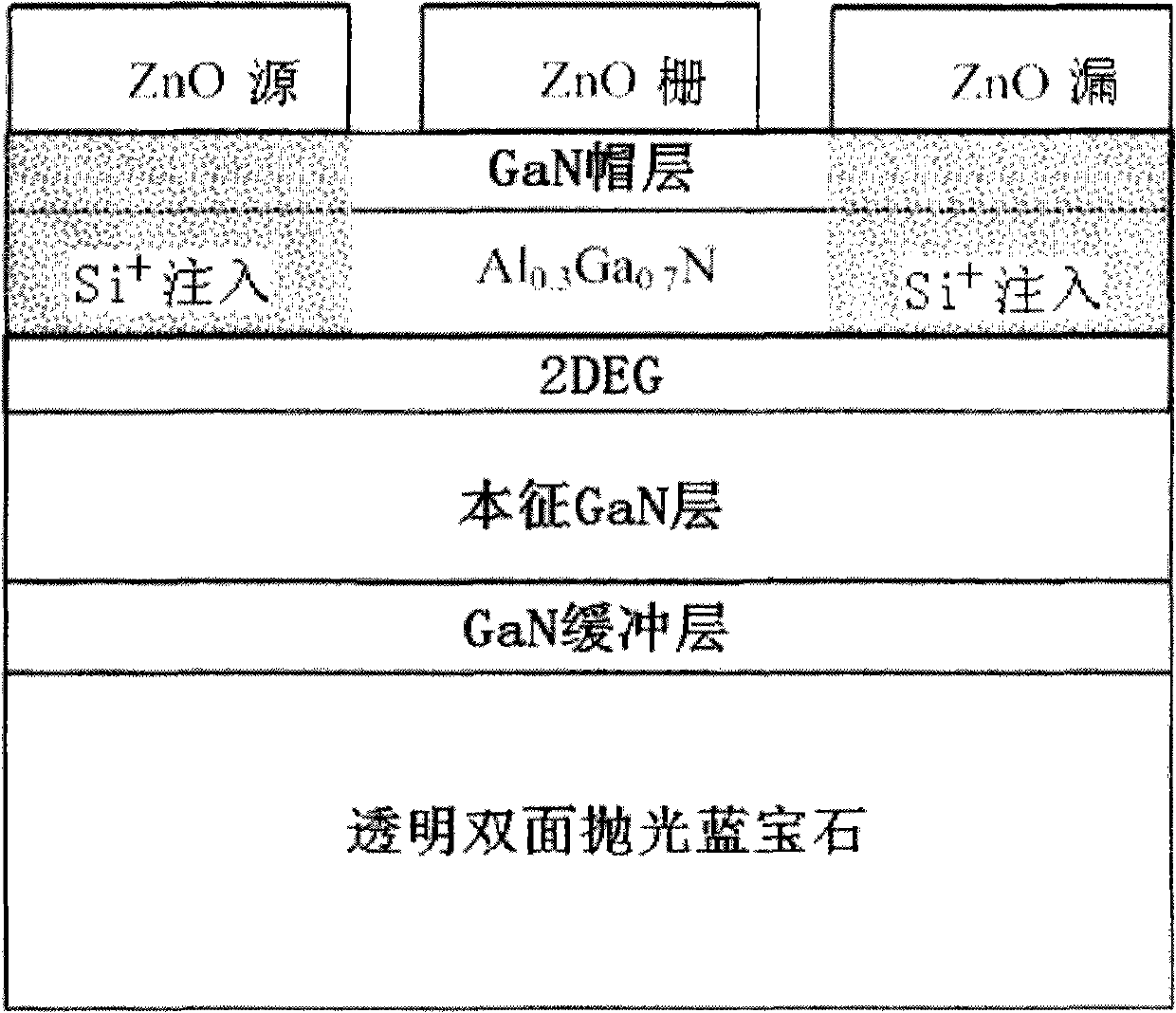
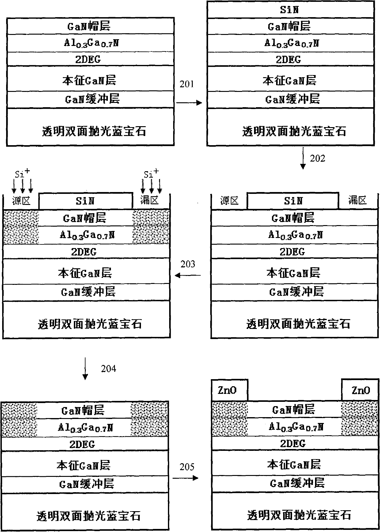
[0034] (101) On the double-sided polished sapphire substrate, grow a GaN buffer layer by MOCVD process;

[0035] (102) growing an intrinsic GaN layer on the GaN buffer layer;

[0036] (103) On the intrinsic GaN layer, a 20nm thick Al 0.3 Ga 0.7 N layer, intrinsic GaN layer and Al 0.3 Ga 0.7 2DEG is formed between N layers;

[0037] (104) in Al 0.3 Ga 0.7 On the N layer, a 2nm thick GaN cap layer is grown.

[0038] Step 2. Fabrication of source and drain electrodes.

[0039] refer to figure 1 and image 3 , the specific implementation of this step is as follows:

[0040] (201) Using PECVD equipment to protect the surface of the device with SiN coverage;

[0041] First, put the sample in acetone for 2 minutes, then in ethan...

Embodiment 2

[0059] Embodiment 2, the making of device of the present invention, comprises the following steps:

[0060] Step 1. Epitaxial material growth.

[0061] refer to figure 1 and figure 2 , the specific implementation of this step is as follows:

[0062] (101) On the double-sided polished sapphire substrate, grow a GaN buffer layer by MOCVD process;

[0063] (102) growing an intrinsic GaN layer on the GaN buffer layer;

[0064] (103) On the intrinsic GaN layer, a 20nm thick Al 0.3 Ga 0.7 N layer, intrinsic GaN layer and Al 0.3 Ga 0.7 2DEG is formed between N layers;

[0065] (104) in Al 0.3 Ga 0.7 On the N layer, a 2nm thick GaN cap layer is grown.

[0066] Step 2. Fabrication of source and drain electrodes.

[0067] refer to figure 1 and image 3 , the specific implementation of this step is as follows:

[0068] (201) Using PECVD equipment to protect the surface of the device with SiN coverage;

[0069] First, put the sample in acetone for 2 minutes, then in ethan...

Embodiment 3

[0087] Embodiment 3, the making of device of the present invention, comprises the following steps:

[0088] Step 1. Epitaxial material growth.

[0089] refer to figure 1 and figure 2 , the specific implementation of this step is as follows:

[0090] (101) On the double-sided polished sapphire substrate, grow a GaN buffer layer by MOCVD process;

[0091] (102) growing an intrinsic GaN layer on the GaN buffer layer;

[0092] (103) On the intrinsic GaN layer, a 20nm thick Al 0.3 Ga 0.7 N layer, intrinsic GaN layer and Al 0.3 Ga 0.7 2DEG is formed between N layers;

[0093] (104) in Al 0.3 Ga 0.7 On the N layer, a 2nm thick GaN cap layer is grown.

[0094] Step 2. Fabrication of source and drain electrodes.

[0095] refer to figure 1 and image 3 , the specific implementation of this step is as follows:

[0096] (201) Using PECVD equipment to protect the surface of the device with SiN coverage;

[0097] First, put the sample in acetone for 2 minutes, then in ethan...


PUM


Abstract

The invention discloses an AlGaN/GaN high electron mobility transistor taking transparent low-resistivity ZnO as a grate electrode, a source electrode and a drain electrode and a manufacturing method thereof, which relate to the field of microelectronic technology and mainly solve the problems that the conventional AlGaN/GaN high electron mobility transistor cannot be used in the field of full transparence and the conventional full transparent transistor has poor characteristics. The transistor sequentially comprises a GaN buffer layer, an intrinsic GaN layer, an Al0.3Ga0.7N layer, a GaN cap layer, the source electrode, the drain electrode and the gate electrode according to the growth sequence, wherein all the source electrode, the drain electrode and the gate electrode are made of a transparent ZnO material doped with Al2O3; an underlay is made of a sapphire with two polished sides; the source electrode, the drain electrode and the gate electrode are deposited on the GaN cap layer by a megnetron sputtering method; and Si+ ions are implanted into a source area and a drain area to assist an ohmic contact formation between the source area and the drain area. The full transparent AlGaN/GaN high electron mobility transistor has the advantages of full transparence and high characteristics, and can be used for electronic elements in an anti-radioactive circuit in the field of transparence.

Description

technical field [0001] The invention belongs to the technical field of microelectronics and relates to semiconductor devices, in particular to a structure and realization of an AlGaN / GaN high electron mobility transistor using transparent low-resistivity material ZnO as the gate, source and drain electrodes, and transparent sapphire as the substrate The method is mainly used to make high-performance devices in the fully transparent field. Background technique [0002] Transparent thin film transistor TTFT (Transparent Thin Film Transistor) has practical and potential wide applications in the fields of flat display, optical information processing, aerospace, military and so on. Using transparent transistors to make transparent integrated circuits, and embedding them in the glass of houses and vehicles, a system with a new information transmission method can be developed, combined with flat-panel display technology to form an integrated electronic information system, which can...

Claims


Application Information

Patent Timeline
Patent Type & Authority Applications(China)
IPC IPC(8): H01L29/778H01L29/43H01L21/335
Inventor 王冲郝跃马晓华张进城曹艳荣杨凌
Owner 云南凝慧电子科技有限公司
Why Eureka
Try Eureka