Layout structure of transverse power components

A technology of lateral power devices and layout structure, applied in the direction of semiconductor devices, electrical components, circuits, etc., can solve the problems of non-uniform turn-on and turn-off, insufficient area utilization, complicated design of curvature terminal parts, etc., to avoid complexity, The effect of compact layout and increased switching speed

Inactive Publication Date: 2010-07-07
UNIV OF ELECTRONIC SCI & TECH OF CHINA
View PDF0 Cites 12 Cited by
  • Summary
  • Abstract
  • Description
  • Claims
  • Application Information

AI Technical Summary

Problems solved by technology

[0005] The technical problem to be solved by the present invention is to provide a horizontal power device layout structure with Compact layout, no need for additional curvature terminal design, l

Method used


Image

  • Layout structure of transverse power components
  • Layout structure of transverse power components
  • Layout structure of transverse power components

Examples


Embodiment Construction

[0026] In order to make the technical problems, technical solutions and beneficial effects to be solved by the present invention clearer, the present invention will be further described in detail below in conjunction with the accompanying drawings and embodiments. It should be understood that the specific embodiments described here are only used to explain the present invention, not to limit the present invention.

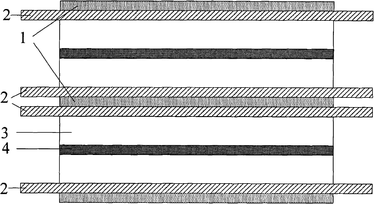
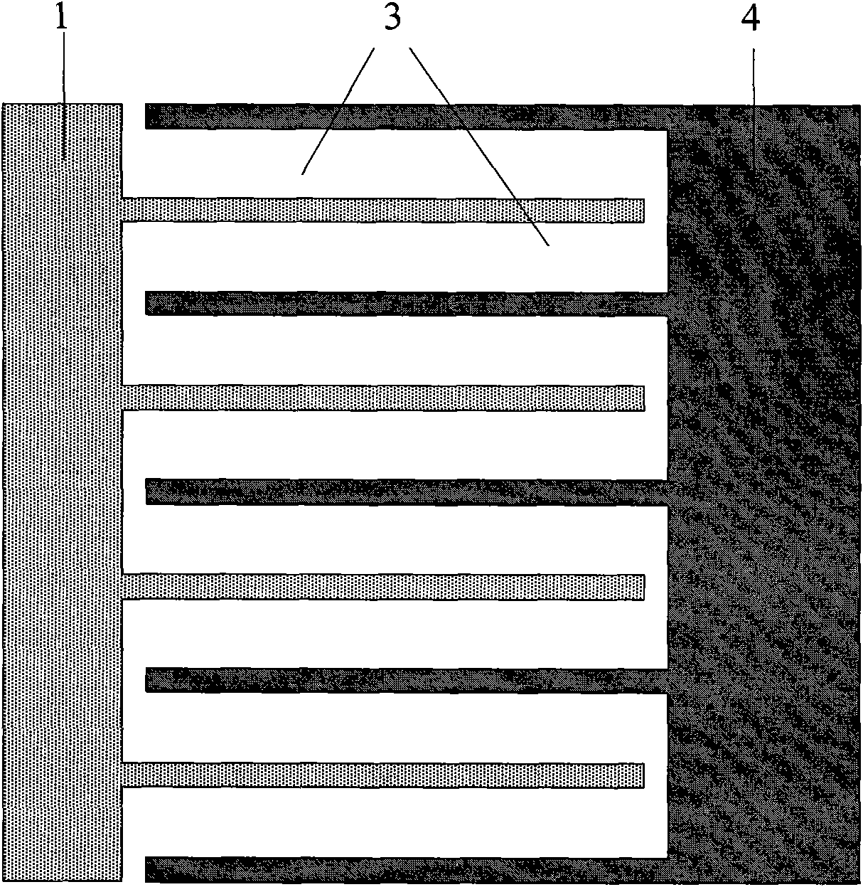
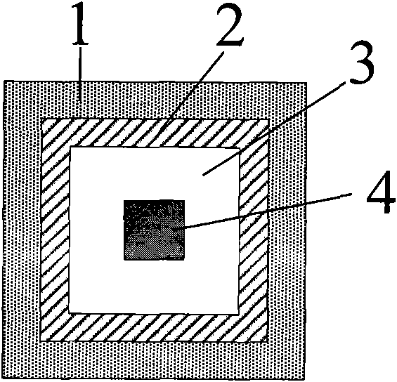
[0027] The invention provides a layout structure of a lateral power device, which adopts a cell arrangement mode for the lateral power device. Compared with the conventional interdigital layout structure, the cell arrangement provides smaller specific on-resistance, and its gate-to-drain Miller capacitance is greatly reduced, which can greatly increase the switching frequency of the device. In addition, the lateral power device layout structure provided by the present invention does not need to increase the curvature terminal because the high-voltage drain electrod...


PUM


Abstract

The invention relates to a layout structure of transverse power components and belongs to the technical field of semiconductor power components. The power components form a cellular arrangement structure on the transversal section; each cellular has the same structure and is provided with the following elements from inside to the outside: a drain electrode, a light dope drift area, a gate electrode and a source electrode, and the drain electrode is enclosed by the light dope drift area, the light dope drift area is enclosed by the gate electrode, and the gate electrode is enclosed by the source electrode; and the transversal sections of each source electrode, gate electrode, light dope drift area and drain electrode of each cellular are of the same shape, and are round or positive n polygons, wherein n is more than or equal to 3. The invention has the advantages of compact layout without additional curvature terminal design, has low on-resistance, small parasitic capacitance, quick switching speed, strong current capacity and the like, and can be used in the layout structure of the transverse power components such as LDMOS, LIGBT and the like.

Description

technical field [0001] The invention belongs to the technical field of semiconductor power devices, and relates to a layout structure of a lateral high-voltage power semiconductor device. Background technique [0002] In integrated circuit design, the layout structure of devices often becomes the key to determine the performance of integrated circuits. A compact and reasonable layout can increase the stability of the integrated circuit and prevent chip failure. A poor layout structure will not only cause a huge waste of chip area, but also cause latch-up effects in integrated circuits, local hot spots in devices, etc., resulting in short chip life and low yield. [0003] Lateral power devices are widely used in power integrated circuits (Power IC, PIC) due to their advantages of wide voltage application range and ease of integration. The layout of lateral power devices often adopts an interdigitated structure. figure 1 A schematic diagram of the layout structure of a tradi...

Claims


Application Information

Patent Timeline
IPC IPC(8): H01L29/78H01L29/739
Inventor 乔明胡曦罗波叶俊蒋苓利傅达平段双亮张波
Owner UNIV OF ELECTRONIC SCI & TECH OF CHINA
Why Eureka
Try Eureka