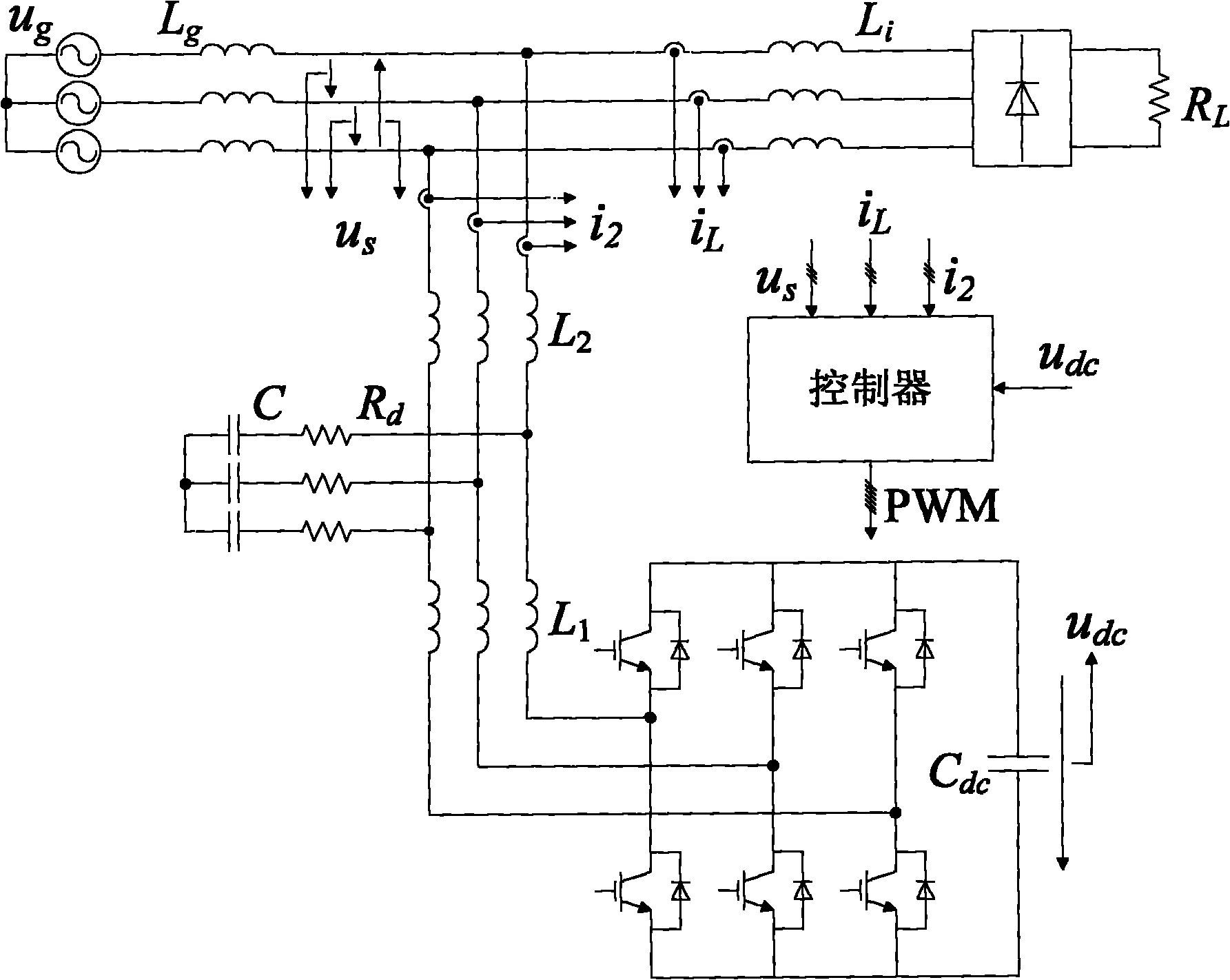
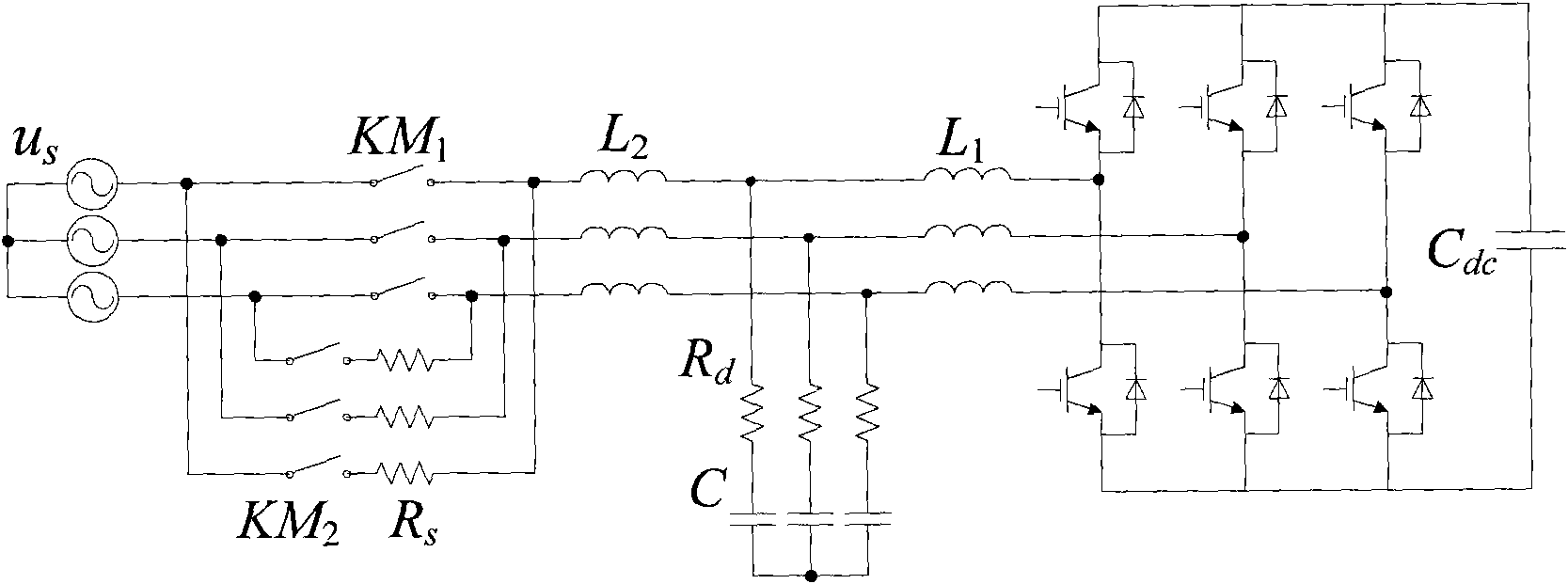
[0049] Embodiment: A method for controlling dynamic DC voltage of a parallel active power filter, characterized in that:
[0050] Step 1, the charging current from the grid precharges the DC side capacitor through the contactor, current limiting resistor, grid side inductance, converter side inductance, and uncontrolled rectifier bridge; this step 1 further includes the following steps: Step 1-1 1. The pre-charging contactor KM2 is closed and the main contactor KM1 is disconnected. Under the action of the grid voltage, the charging current passes through the pre-charging contactor KM2, current limiting resistor, grid-side inductance, converter-side inductance, and uncontrolled rectifier bridge. , and finally flows into the DC capacitor, the DC voltage continues to rise until the charging current is close to zero, and the DC voltage reaches a stable value Udc1; step 1-2, after the charging is stable, the main contactor KM1 is closed, the current limiting resistor Rs and the pre- The charging contactor KM2 is short-circuited by the main contactor KM1, and the charging current passes through the pre-charging contactor KM1, grid-side inductance, converter-side inductance, uncontrolled rectifier bridge, and finally flows into the DC capacitor, and the DC voltage continues to rise until the charging current Close to zero, the DC voltage reaches a stable value Udc2; the uncontrolled rectifier bridge is composed of a main switch tube and an anti-parallel diode.
[0051] Step 2. The switch of the lower bridge arm of the uncontrolled rectifier bridge is turned off by the pulse signal sent by the controller, and the switch of the upper bridge arm of the uncontrolled rectifier bridge is turned on under the control of the switch pulse signal sent by the controller. The switch pulse signal The duty cycle increases linearly from 0 to a fixed value; then the DC capacitor is continuously charged at the fixed value.
[0052] Step 3. Turn off the switch of the lower bridge arm and the switch of the upper bridge arm at the same time, and the charging current will be stored in the grid side inductor, The energy in the converter side inductance is transferred to the DC side capacitor in the form of charging current through the anti-parallel diode of the uncontrolled rectifier bridge until the voltage of the DC side capacitor reaches the desired voltage value; the desired voltage value is 700V.
[0053] Step 4. Place the PI controller in the current loop in the d-q synchronous coordinate system, and set the initial output value of the PI controller; the initial output value of the PI controller is -35 or 27.
[0054] Step 5, adding the sampled value of the grid voltage to the output value of the PI controller in the PI control inner loop in the current loop after being calculated by Gn(s), and the added value forms a set of modulation signals through d-q inverse transformation , the modulation signal is compared with the triangular wave modulation signal inside the controller to obtain a set of PWM pulse signals. The PWM pulse signal controls or not controls the switch in the rectifier bridge, so that the output is basically the same as the grid voltage and the phase is used to suppress the DC side. Three-phase AC voltage with capacitor voltage fluctuations; G n (s) The formula is as follows:
[0055] G n ( s ) = L 1 Cs 2 + CR d s + 1 L 1 Cs 2 / 10 + ( CR d + L 1 / 10 R d ) s + 1
[0056] By system parameters: L 1 is the inductance, the unit is mH; C is the capacitance, the unit is uF; R d Damping resistance, in Ω.
[0057] Step 6. Set a repetitive controller in the repetitive control outer loop of the current loop, and delay the repetitive controller for a certain characteristic time in the repetitive control outer loop to delay the input time of the repetitive controller. The characteristic time should be greater than The duration of the grid-connected shock is greater than half of the fundamental cycle time.
[0058] Step 7. Eliminate voltage harmonics in the power grid through a low-pass filter in the voltage loop.
[0059] The above content of this embodiment is explained in detail as follows.
[0060] 1. DC side capacitor pre-charging
[0061] The purpose of pre-charging is to make the DC capacitor voltage rise smoothly from 0 to a certain voltage value. The precharging process of the DC link voltage is as follows: figure 2 shown. It is realized by an uncontrolled rectifier bridge composed of anti-parallel diodes of the main switching tube. In order to limit the inrush current of the grid to the DC capacitor, a suitable current-limiting resistor Rs is connected in series with the grid-side inductance L2. Since the capacitive reactance of the AC filter capacitor C is very large at the fundamental frequency of the power grid, the analysis can be considered as an open circuit and not considered.
[0062] The specific implementation method of pre-charging is as follows: the pre-charging contactor KM2 is closed and the main contactor KM1 is opened. The inductance and uncontrolled rectifier bridge finally flow into the DC capacitor, and the DC voltage continues to rise until the charging current is close to zero, and the DC voltage reaches a stable value Udc1. After the charging is stable (that is, the charging current is close to zero), the main contactor KM1 is closed, the current limiting resistor Rs and the pre-charging contactor KM2 are short-circuited by the main contactor KM1, and the charging current passes through the pre-charging contactor KM1 and the grid-side inductor successively. , converter side inductance, uncontrolled rectifier bridge, and finally flow into the DC capacitor, the DC voltage continues to rise until the charging current is close to zero, and the DC voltage reaches a stable value U dc2.
[0063] u dc1 and U dc2 Calculated as follows:
[0064] After the charging is stable, the charging current flowing through L1 is almost zero, and the voltage value of the DC capacitor depends on Rs, L 2 , R d The effective value of the voltage of the AC filter capacitor C in the second-order circuit composed of C and C. The voltage value of the DC capacitor can be calculated as follows:
[0065] U dc 1 = 2 X c X c 2 + R s 2 U g . - - - ( 1 )
[0066] Among them, U dc1 ,Xc,U g Respectively represent the DC capacitor voltage value after the current limiting resistor is connected in series and the charge is stable, the capacitive reactance value of the AC filter capacitor C, and the effective value of the grid voltage.
[0067] U dc 2 = 2 U g . - - - ( 2 )
[0068] In order not to produce excessive voltage step impact, it is usually required
[0069] u dc1 ≥0.9U dc2.(3)
[0070] The maximum value of the current-limiting resistance can be determined by formula (3), and the minimum value depends on the maximum surge current that the switching tube IGBT of the converter can accept during the pre-charging process.
[0071] The details are as follows: The parameters of the actual system are as follows: Xc=26.54Ω, U dc2 = 537.32, U dc1 ≥483.59V, you can get Rs≤12.85Ω. According to the ability of each component to withstand the impact current at the moment of charging and retain a certain margin, the maximum acceptable impact current is taken as 100A, and Rs≥220V/100A=2.2Ω is roughly calculated. Considering the reliable protection of the components at the moment of power-on, choose a larger resistance value as much as possible and combine the actual power resistance value that can be purchased, and finally Rs is taken as 10Ω.
[0072] 2. DC side capacitor chopper boost
[0073] The pre-charging of the DC side capacitor can make the voltage of the DC capacitor rise to U dc2 , if the grid voltage U g =380V, U dc2 =540V, which is still far from the steady-state value of 700V required by the system, and the capacitor voltage can be gradually increased from 540V to 700V through the chopper boost process.
[0074] The process of chopper boost is shown in Fig. 3(a) and (b). Since the capacitive reactance of the AC filter capacitor C is very large at the fundamental frequency of the power grid, the analysis can be considered as an open circuit and not considered. Grid side inductance L 2 and converter side inductance L 1 Formed in series to form an equivalent inductance L.
[0075] The specific implementation method of chopper boost is as follows: figure 1 The pulse signal sent by the controller DSP in the circuit turns off the No. 2, No. 4 and No. 6 IGBTs of the three lower bridge arms, and applies the same switching pulse signal to the No. 1, No. 3 and No. 5 IGBTs of the three upper bridge arms. Figure 3(a) shows the charge current flow when No. 2, No. 4 and No. 6 IGBTs of the lower bridge arm are turned off, and No. 1, No. 3 and No. 5 IGBTs of the upper bridge arm are turned on at the same time. Under the action of the grid voltage, the charging current passes through the equivalent series inductance and the three IGBTs of the upper bridge arm to form a closed loop. The charging current stores energy for the equivalent series inductance L, but does not charge the DC capacitor. Figure 3(b) shows the charge current flow when IGBTs 2, 4, and 6 of the lower bridge arm are turned off, and IGBTs 1, 3, and 5 of the upper bridge arm are turned off at the same time. Under the combined effect of grid voltage and inductance L, the energy stored in L is transferred to the DC capacitor in the form of charging current through the anti-parallel diodes of No. 1 to No. 6 IGBTs, so that the DC voltage continues to rise.
[0076] The duty cycle of the IGBT switching pulse signals of the three upper bridge arms 1, 3, and 5 increases linearly from 0 to a fixed value; then the DC capacitor is continuously charged at the fixed value until the controller DSP detects that the DC capacitor voltage reaches The expected value is 700V. The duty cycle step and the maximum duty cycle are adjusted according to the actual required DC capacitor charging time and the maximum current that the switch tube can withstand.
[0077] The details are as follows: through figure 1 The pulse signal sent by the controller DSP in the circuit turns off the No. 2, No. 4 and No. 6 IGBTs of the three lower bridge arms, and applies the same switching pulse signal to the No. 1, No. 3 and No. 5 IGBTs of the three upper bridge arms. The stepping and maximum duty cycle of the three upper bridge arms 1, 3, and 5 IGBTs are adjusted according to the actual required DC capacitor charging time and the maximum current that the switch tube can withstand. The value of the maximum duty cycle can be gradually increased on the basis of exceeding the duty cycle of the dead zone. The actual system dead zone time is 0.0033ms, the switching period is 0.142ms, and the dead zone duty cycle is 2.3%. The duty cycle step and the maximum duty cycle are adjusted according to the charging time during the experiment and the impact current on the AC side. The final maximum duty cycle is taken as 10%, and the duty cycle step is increased by 1% every 1ms, that is, in the preset Based on the stable charging voltage of 537V, the duty cycle increases from 0% every 1ms to 10% by 1% every 1ms, and then chopper boosts with a fixed duty cycle of 10% until the DC voltage rises to the desired value of 700V.
[0078] 3. DC side capacitor voltage grid-connected impact suppression
[0079] After the DC voltage reaches 700V through the DC side capacitor chopper step-up, the system is about to enter the compensation state and run stably. However, at the moment when the device starts to work, the DC side voltage will fluctuate greatly. The impact suppression method of this patent can realize that the DC capacitor voltage has no impact during the grid connection process, and basically maintains at 700V.
[0080] The specific implementation method of DC side capacitor voltage grid-connected impact suppression is as follows:
[0081] First put Figure 4The current loop PI controller in is placed in the d-q synchronous coordinate system, and the initial output value of the PI controller is set. The initial value can be directly set as the d-q forward transformation value of the grid voltage, or can be determined through simulation and experiment.
[0082] followed by Figure 4 The grid voltage in is fed forward to the output of the current loop PI controller through Gn(s). The sampled value of the grid voltage is introduced into the output point of the current loop PI controller after calculation with Gn(s), the calculated value is added to the output value of the current loop PI controller, and the added value is formed by d-q inverse transformation A set of modulation signals, the modulation signal is compared with the triangular wave modulation signal inside the controller DSP to obtain a set of PWM pulse signals, through which the output of the 6 IGBT switch tubes of the converter is controlled and the magnitude and phase of the grid voltage are basically The same three-phase AC voltage. The three-phase AC power output by the converter can basically offset the grid voltage, and can suppress the fluctuation of the DC capacitor voltage to a large extent.
[0083] Figure 4 Among them, Gn(s) is designed as follows. The influence of the grid voltage on the output compensation current can be expressed as follows:
[0084] i 2 ( s ) u g ( s ) = G n ( s ) G p ( s ) - 1 ( L 2 + L g ) s + [ L 1 s + PI ( s ) ] G p ( s ) - - - ( 4 )
[0085] in
[0086] G p ( s ) = 1 + CR d s L 1 Cs 2 + CR d s + 1 . - - - ( 5 )
[0087] The negative effect of grid voltage can be completely eliminated when the following conditions are met:
[0088] G n ( s ) = 1 / G p ( s ) = L 1 Cs 2 + CR d s + 1 CR d s + 1 . - - - ( 6 )
[0089] However, since the order of the numerator in the above formula is greater than the order of the denominator, the above formula cannot be realized physically. Considering the physical implementation problem, it is usually sufficient to achieve full compensation within the main frequency band, and formula (6) can be modified as
[0090] G n ( s ) = L 1 Cs 2 + CR d s + 1 ( CR d s + 1 ) ( T n s + 1 ) = L 1 Cs 2 + CR d s + 1 CR d T n s 2 + ( CR d + T n ) s + 1 , L 1 C CR d T n . - - - ( 7 )
[0091] In practice, the time constant can be taken as
[0092] T n = L 1 /10R d. (8)
[0093] The final form of Gn(s) can be taken as
[0094] G n ( s ) = L 1 Cs 2 + CR d s + 1 L 1 Cs 2 / 10 + ( CR d + L 1 / 10 R d ) s + 1 . - - - ( 9 )
[0095] Finally, after including Figure 5 In the system of the repeated control outer loop and the PI control inner loop shown, the negative influence of the repetitive controller on the error accumulation at the moment of grid connection should be further eliminated. Figure 5 The transfer function of the internal model of the repeated controller in is as follows:
[0096] G im ( z ) = e 0 ( z ) e i ( z ) = 1 1 - Q ( z ) z - N - - - ( 10 )
[0097] Among them, Q(z) is a constant slightly smaller than 1, which is taken as 0.9 in this system.
[0098] According to formula (10), the difference equation of the internal model can be obtained
[0099] e 0 (k)=e i (k)+0.9e 0 (k-N) (11)
[0100] Equation (11) shows that the internal model accumulates the input error signal at each fundamental cycle until the error is less than 0.9 times the output signal.
[0101] In the current loop program, a specific time-delay program is designed to delay the input time of the repetitive controller. During the delay process, only the inner loop of the PI control works, and the outer loop of the repetitive control does not make any adjustments to the system error. The delay time should be greater than the duration of the grid-connected shock, usually greater than half of the fundamental cycle time. It is also possible to design a delay program in the current loop program to increase slowly periodically Figure 5 The Q(z) value in . In the process of slowly increasing Q(z), both loops of the system are in working condition, PI controls the inner loop to work normally, repeats the control of the outer loop to slowly and weakly adjust the error according to the size of Q(z), and when Q(z) increases After reaching the steady-state set value, the outer loop of repeated control also enters the normal working state. The increase time of Q(z) should usually be greater than half of the fundamental cycle time.
[0102] The details are as follows: First, the Figure 4 The current loop PI controller in is placed in the d-q synchronous coordinate system, and the initial output value of the PI controller is set. The initial value can be directly set as the d-q forward transformation value of the grid voltage. The size of the initial value of PI can also be roughly determined through simulation and experiments. First, determine the initial value of PI in the program according to the steady-state output average value of current loop and voltage loop PI in simulation software such as Matlab. The initial values of PI in the dq coordinate system of the system at rated capacity are: -30 and 25 respectively. The negative initial value of the d-axis means that the converter absorbs active power from the grid to stabilize the DC side voltage. The final initial value of PI is determined according to the experiment, and the initial value of PI in the experiment is -35 and 27 respectively. followed by Figure 4 The grid voltage in is fed forward to the output of the current loop PI controller through Gn(s). Considering the problem of physical realization, it is usually enough to realize full compensation in the main frequency band, and the final form of Gn(s) can be taken as
[0103] G n ( s ) = L 1 Cs 2 + CR d s + 1 L 1 Cs 2 / 10 + ( CR d + L 1 / 10 R d ) s + 1 . - - - ( 16 )
[0104] By system parameters: L 1 =0.056mH, C=120uF, R d =0.1Ω, take
[0105] T n =L 1 /10R d =5.6000e-005
[0106] The designed Gn(s) can be obtained from formula (10)
[0107] G n ( s ) = 6.72 e - 009 s 2 + 1.2 e - 005 s + 1 6.72 e - 010 s 2 + 6.8 e - 005 s + 1 - - - ( 17 )
[0108] For the sake of simplicity and convenience, Gn(s) can be taken as 1, that is, to achieve full compensation in steady state.
[0109] Finally, a specific time-delay program is designed in the current loop program to delay the input time of the repetitive controller. During the delay process, only the inner loop of the PI control works, and the outer loop of the repetitive control does not make any adjustments to the system error. The delay time should be greater than the duration of the grid-connected impact, usually greater than or equal to half the fundamental wave cycle time, the system design delay is 10ms. It is also possible to design a delay program in the current loop program to increase slowly periodically Figure 5 The Q(z) value in . In the process of slowly increasing Q(z), both loops of the system are in working condition, PI controls the inner loop to work normally, repeats the control of the outer loop to slowly and weakly adjust the error according to the size of Q(z), and when Q(z) increases After reaching the steady-state set value, the outer loop of repeated control also enters the normal working state. The increase time of Q(z) should usually be greater than half of the fundamental cycle time. In this system, Q(z) increases periodically from 0.5 to 0.9 within 10ms.
[0110] 4. Rapid recovery of DC side capacitor voltage
[0111] After the grid-connected impact is suppressed by the capacitor voltage on the DC side, the system enters steady-state operation, and the DC voltage remains stable. However, during load switching, the DC capacitor voltage will fluctuate greatly. The method of this patent can realize the rapid recovery of the DC capacitor voltage during the load switching process.
[0112] According to the balance equation, the small-signal model of DC voltage control can be derived as Image 6 shown. The block diagram of voltage loop closed-loop control with controller F(s) is as follows: Figure 7 shown
[0113] The open-loop transfer function of the system is:
[0114] M ( s ) = 3 U s - 6 RI p - 3 LI p s C dc U dc s F ( s ) . - - - ( 12 )
[0115] Among them, R is the equivalent resistance including the loss of LCL filter and converter, I p is the effective value of the active current on the AC side. The transfer function of the traditional PI controller is:
[0116] F PI ( s ) = K p + K i s . - - - ( 13 )
[0117] Among them, Kp and Ki are the proportional and integral coefficients of the voltage loop PI controller, respectively.
[0118] The Bode diagrams of the open-loop transfer function M(s) of the system without a controller and with a PI controller are shown in Fig. 8(a), respectively. It can be seen from 8(a) that the frequency characteristic curves of the two are very similar, but the low frequency gain is slightly different. Although the phase margin of the system is large in both cases, the attenuation performance of the high-frequency part is not ideal, which is not conducive to suppressing the noise in the loop. An ideal controller should have high-frequency attenuation capability while ensuring sufficient low-frequency gain.
[0119] The voltage outer loop controller keeps the DC side voltage constant by adding appropriate active current to the command signal of the current inner loop. Since the output compensation current is 6n±1 order harmonic current, there will be 6n order voltage harmonics on the DC side. When the voltage loop adopts the traditional PI controller, these harmonics will also exist in the output of the controller, which will greatly interfere with the normal operation of the current loop. When the capacitance value is small, the large harmonic voltage will seriously interfere with the normal operation of the current loop and seriously affect the compensation accuracy.
[0120] Replacing the traditional PI controller with a low-pass filter to eliminate these voltage harmonics seems to be a viable approach. Obviously, when having the same bandwidth as the PI controller, the low-pass filter can obtain better compensation accuracy. In other words, under the condition of ensuring the same compensation accuracy, the bandwidth of the voltage loop can be expanded when the low-pass filter is used, thereby improving the dynamic response speed of the voltage loop. In addition, the steady-state tracking capability of the DC voltage can be guaranteed by the integral link (1/sCdcUdc) inside the model. First-order and second-order low-pass filters are easy to stabilize and design, and can be selected as controllers with the following transfer functions:
[0121] F 1 ( s ) = K 1 1 + s / ω c 1 . - - - ( 14 )
[0122] F 2 ( s ) = K 2 ω c 2 2 s 2 + 2 ξ ω c 2 s + ω c 2 2 . - - - ( 15 )
[0123] Among them, K 1 and K 2 are the scale coefficients of the first-order and second-order filters, respectively, ω c1 and ω c2 are the cut-off frequencies of the first-order and second-order filters, respectively, and ξ is the damping coefficient of the second-order filter. The cutoff frequency of the filter depends on the bandwidth required by the design. The gain design should be a compromise between low frequency gain and system stability margin. The damping ratio mainly depends on the desired phase margin and high frequency attenuation performance.
[0124] The working principle diagram of the voltage loop is as follows: Figure 9 shown. In the figure, Ucr is the given value of the DC side voltage, and Ucf is the feedback value of the DC side voltage. The specific implementation method of the fast recovery of the capacitor voltage on the DC side is as follows:
[0125] Controller DSP real-time sampling Figure 9 The instantaneous value of DC capacitor voltage U cf , and then use the steady-state voltage setpoint U cr minus U cf , when U cf Than U cr hour, through the action of the first-order or second-order filter, making Δi d is positive, by Figure 9It can be seen that the command current finally obtained after calculation will contain positive active current components. Under the action of this command current, the main circuit of the compensator will absorb the corresponding active power from the grid while compensating the harmonic current, so that The DC side capacitor voltage of the converter rises until the feedback voltage is the same as the given value.
[0126] Conversely, when U cf Than U cr When it is large, through the action of the first-order or second-order filter, Δi d negative, the command current finally obtained after calculation will contain a negative active current component. Under the action of this command current, the main circuit of the compensator will release the corresponding active power to the grid while compensating the harmonic current , so that the DC side capacitor voltage of the converter drops until the feedback voltage is the same as the given value.
[0127] The details are as follows: the first-order and second-order low-pass filters are easy to stabilize and design, and can be selected as controllers, and their transfer functions are shown in formulas (7) and (8). In this system, the cut-off frequency and gain of the first-order filter are set to 85Hz, 3, and the cut-off frequency, gain and damping ratio of the second-order filter are set to 66Hz, 3 and 2, respectively. The Bode plots of M(s) with a first-order filter and a second-order filter are shown in Figure 8(b), respectively. It can be seen from Figure 8(b) that the two attenuate the harmonics of the DC side voltage at -20dB/dec and -40dB/dec respectively in the high frequency band. The phase margins of the two are 45° and 30° respectively, which is sufficient for the stability of the whole system. In addition, compared with the first-order filter, the second-order filter has a higher high-frequency attenuation rate, which is beneficial to obtain a better compensation effect. However, second-order filters have a slightly lower bandwidth, so the response is correspondingly slower. In general, although the phase margin of the system with the first-order and second-order filters is lower than that of the PI, they can achieve better DC voltage control performance. The main performance comparison of the system when using different controllers is shown in Table 1.
[0128] Table 1 The main performance comparison of the system when using different controllers
[0129]
[0130] 5. Simulation results