Method for manufacturing embedded high-conductivity printed circuit board (PCB)

A technology of PCB board and manufacturing method, applied in multilayer circuit manufacturing, printed circuit manufacturing, electrical components and other directions, can solve the problems of PCB high frequency signal influence, complex welding process, large electrical signal transmission loss, etc. The effect of power miniaturization PCB design, simple production process and stable heat dissipation performance

Active Publication Date: 2010-07-28
DONGGUAN SHENGYI ELECTRONICS
View PDF0 Cites 56 Cited by
  • Summary
  • Abstract
  • Description
  • Claims
  • Application Information

AI Technical Summary

Problems solved by technology

The traditional method is to attach a large metal heat dissipation substrate on the back of the entire circuit board. Larger, increasing the space occupied by the whole device
In addition, the traditional metal substrate uses a whole piece of copper or aluminum, which not only wastes materials and has a great impact on the environment, but also the whole piece of metal has an impact on PCB high-frequency signals, which is not suitable for wireless microwave products

Method used


Image

  • Method for manufacturing embedded high-conductivity printed circuit board (PCB)
  • Method for manufacturing embedded high-conductivity printed circuit board (PCB)
  • Method for manufacturing embedded high-conductivity printed circuit board (PCB)

Examples


Embodiment Construction

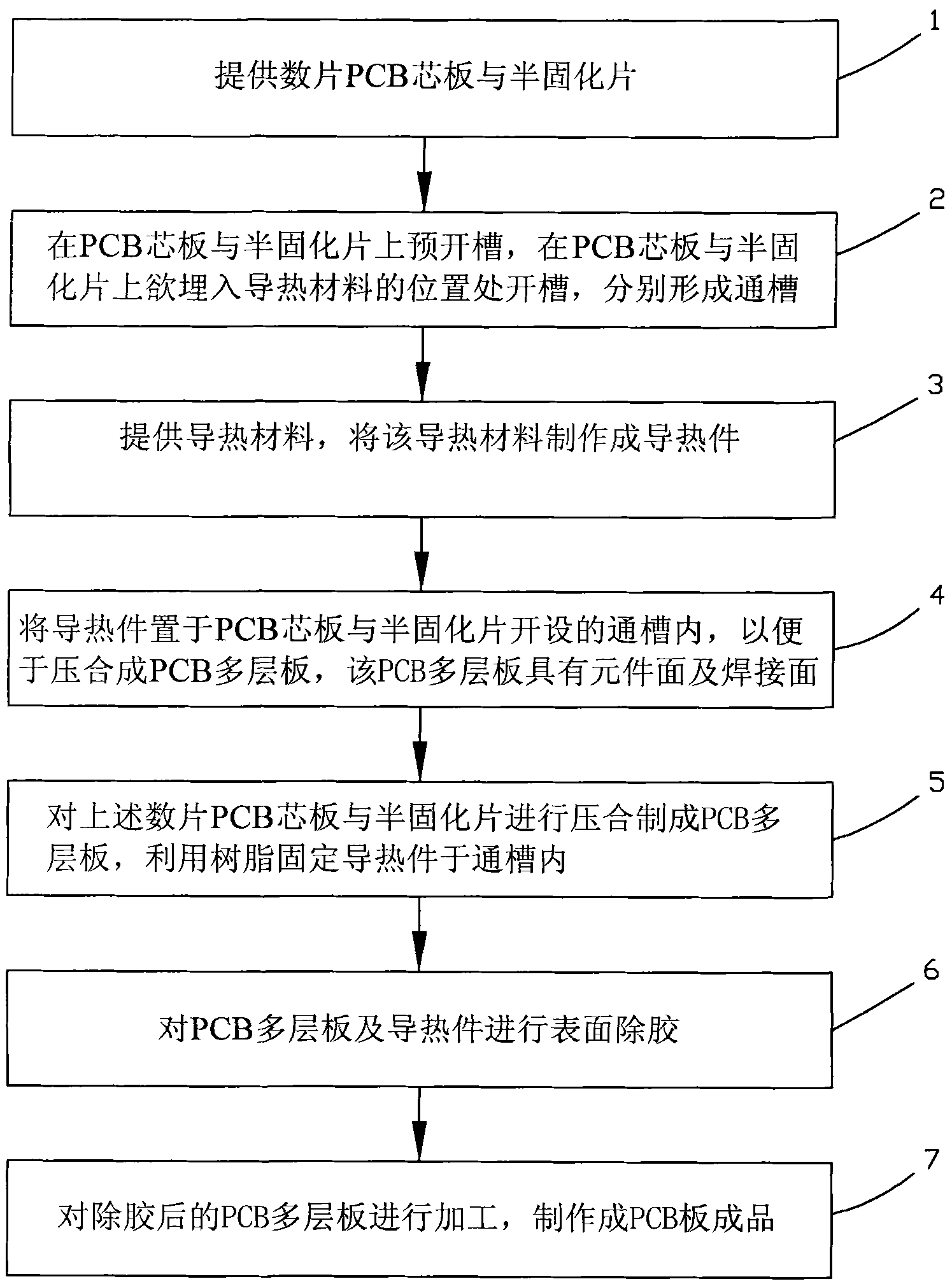
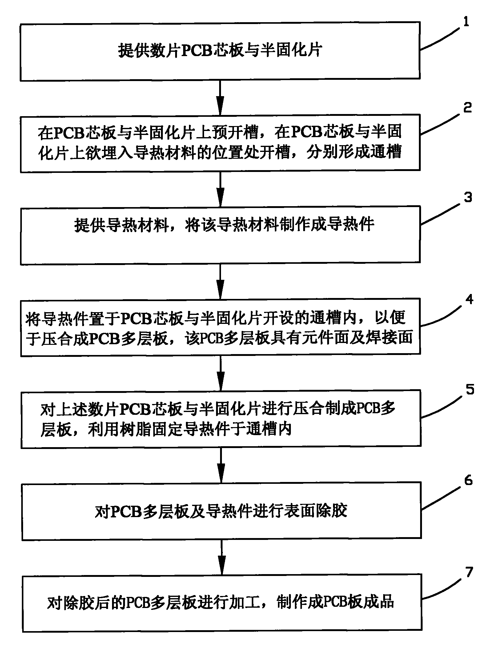
[0025] Such as Figure 1-2 Shown, the manufacture method of embedded type high thermal conductivity PCB board of the present invention, it comprises:

[0026] Step 1. Provide several PCB core boards and prepregs. The PCB core board and prepreg can be provided by existing technology, wherein one or more layers of materials are made of low dielectric constant (LOW Dk) materials, for example, the commercially available models are Ro4350, Ro3003, or RF35-A2, etc. Material.

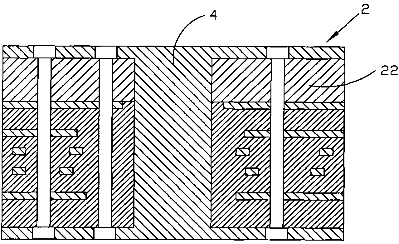
[0027] Step 2. Pre-slot on the PCB core board and the prepreg. Slots are made on the PCB core board and the prepreg where the heat-conducting material is to be embedded to form through grooves respectively, and the core board and the prepreg have matching positioning holes.

[0028] Step 3, providing a thermally conductive material, and making the thermally conductive material into a thermally conductive member 4 . In the embodiment of the present invention, the heat conducting element is a rectangular par...


PUM


Abstract

The invention discloses a method for manufacturing an embedded high-conductivity printed circuit board (PCB). The method comprises the following steps of 1, providing a plurality of PCB core boards and prepregs; 2, pre-slotting on the PCB core boards and the prepregs, slotting at positions where conductive materials are to be embedded on the PCB core boards and the prepregs, and respectively forming slots, wherein the core boards and the prepregs have matched positioning holes; 3, providing the conductive materials and manufacturing conductive elements by using the conductive materials; 4, placing the conductive elements in the slots of the PCB core boards and the prepregs for laminating the conductive elements into PCB multi-layer boards which have component faces and welding faces; 5, laminating the plurality of PCB core boards and prepregs to manufacture PCB multi-layer boards and fixing the conductive elements in the slots by using resins; 6, performing degumming on the surfaces of the PCB multi-layer boards and the conductive elements; and 7, processing the PCB multi-layer boards after degumming to obtain PCB finished products. The method has the advantages of simple manufacturing flows and realization of high radiation, high-speed signal transmission and the like by embedding the conductive materials into the PCB in a laminating manner and matching the conductive materials with the thickness of the PCB.

Description

technical field [0001] The invention relates to a method for manufacturing a PCB board, in particular to a method for manufacturing a PCB board with high thermal conductivity by adopting a lamination method. Background technique [0002] With the widespread use of high-frequency electronic signals, the heat generated by the components of the chip on the printed circuit board (PCB), especially the heat generated by the high-power components will cause great damage to the components, which needs to be used Heat dissipation or cooling methods help to dissipate heat energy, so it is necessary to design an effective heat dissipation method on the PCB board to dissipate the high heat generated during the operation of the chip at any time. The traditional method is to attach a large metal heat dissipation substrate on the back of the entire circuit board. Larger size increases the space occupied by the whole device. In addition, the traditional metal substrate uses a whole piece ...

Claims


Application Information

Patent Timeline
Patent Type & Authority Applications(China)
IPC IPC(8): H05K3/46H05K3/00H05K1/02
Inventor 陈立宇袁继旺董浩彬
Owner DONGGUAN SHENGYI ELECTRONICS
Why Eureka
Try Eureka