Patch-type filamentous fuse and manufacturing method thereof
A fuse and chip technology, applied in the field of electronic protection components, can solve the problems of difficulty in producing small or ultra-small fuses, difficult to guarantee compactness, low production efficiency, etc., and achieve stable and reliable processing technology and production costs. The effect of low, production efficiency improvement
- Summary
- Abstract
- Description
- Claims
- Application Information
AI Technical Summary
Problems solved by technology
Method used
Image
Examples
preparation example Construction
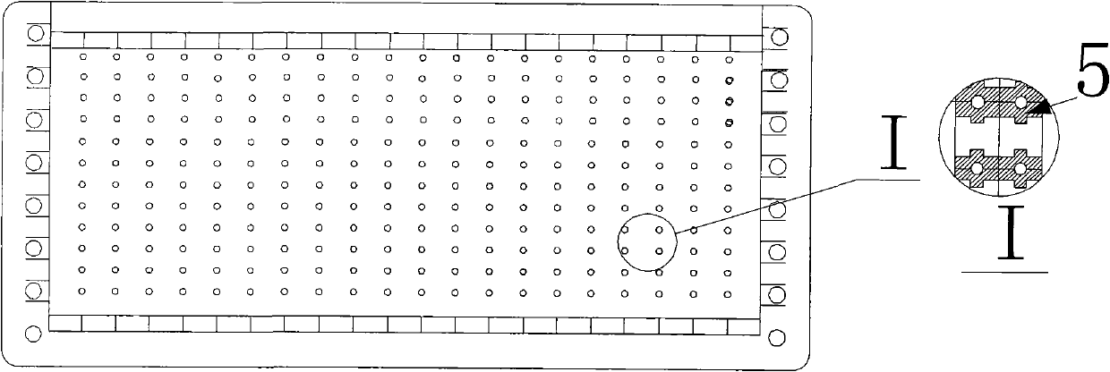
[0023] The preparation of the fuse of the present invention: form a plurality of small cell array substrates (such as figure 2 ), each substrate unit has an independent circuit board that is the same as other units, the circuit board is formed by evaporation, electroplating or etching, and then the fuse is bonded or welded on the surface electrode of the circuit board, The encapsulation material wraps the fuse wire, solder joint or bonding point and part of the surface electrode, and is tightly connected with the substrate, and then the whole substrate is cut to form this product.
[0024] The above-mentioned fuses may be one or more according to different products. Fuse diameters range from 15 microns to 500 microns.
[0025] During production, first clean the substrate 4, remove the dust and dirt on the surface of the substrate in an ultrasonic cleaning machine, place the substrate in a special fixture, and then use ultrasonic pressure welding or solder bonding to bond the...
Embodiment 1
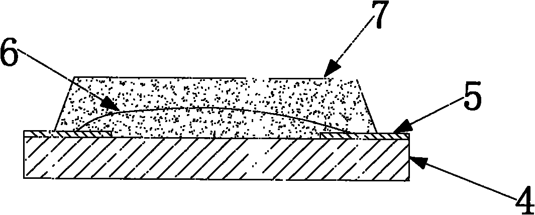
[0028] like image 3 , Figure 4 As shown, a single fuse 6 is welded or bonded to the electrode area 5 of the substrate, and the encapsulation layer 7 wraps the fuse 6 and is closely attached to the substrate 4, ensuring the airtightness of the encapsulation.
Embodiment 2
[0030] like Figure 5 , Image 6 As shown, two fuses 6 are welded or bonded to the electrode area 5 of the substrate, and the encapsulation layer 7 wraps the fuses 6 and is closely attached to the substrate 4, ensuring the airtightness of the encapsulation.
[0031] The performance of the products produced by this process is compared with that of traditional products. The resistance of the products produced by this process is relatively stable. The maximum and minimum resistance values of the same batch of products are within 5 milliohms, and the voltage drop can be controlled within 5%. , and its fusing characteristics are also very consistent, which fully demonstrates the feasibility and advancement of the process.
PUM
 Abstract
Description
Claims
Application Information


