Supercharge Your Innovation With Domain-Expert AI Agents!

Writing system for static random access memory and memory

A writing system and memory technology, applied in static memory, digital memory information, information storage, etc., can solve problems such as inability to effectively reverse data, affect the charging and discharging time of bit lines, and difficult to correctly control the time point

Active Publication Date: 2010-08-18
FARADAY TECH CORP
View PDF2 Cites 4 Cited by
  • Summary
  • Abstract
  • Description
  • Claims
  • Application Information

AI Technical Summary

Problems solved by technology

If a negative pulse voltage is coupled to the bit line before the potential of the bit line is fully discharged to a low potential, the negative pulse voltage will not be able to effectively reverse (flip) the data stored in the memory cell
Due to the drift and change of the process, operating voltage and / or temperature will affect the charging and discharging time of the bit line, and jointly, the time point of introducing the negative pulse voltage becomes difficult to control correctly

Method used


Image

  • Writing system for static random access memory and memory
  • Writing system for static random access memory and memory
  • Writing system for static random access memory and memory

Examples


Embodiment Construction

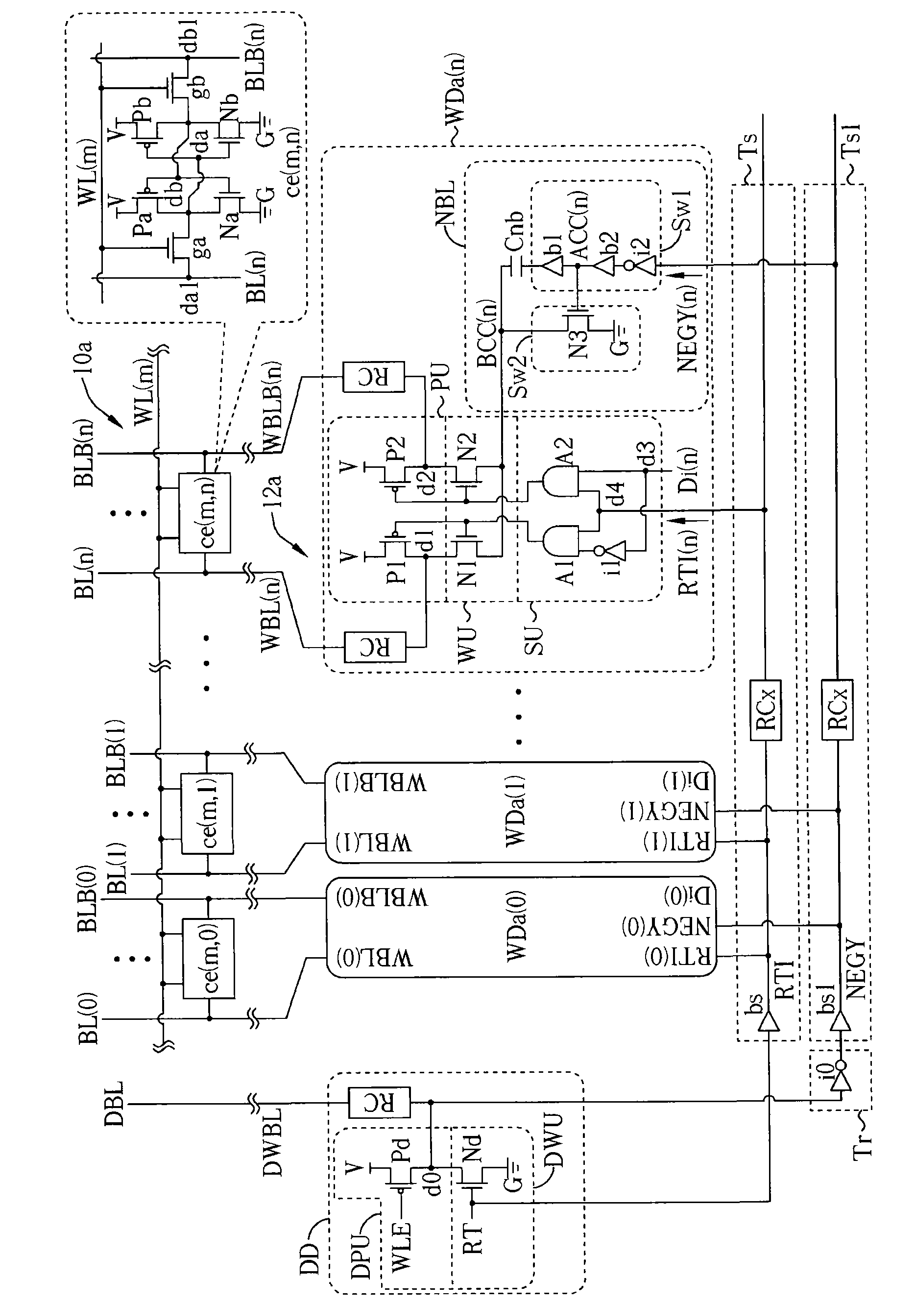
[0074] Please refer to figure 1 , which shows a schematic circuit diagram of an embodiment 10a of the memory of the present invention. In this embodiment, the memory 10a may be a static random access memory, which has a plurality of memory cells arranged in a matrix; for the memory cells on the mth row that are commonly coupled to the word line WL(m), it includes The memory cell ce(m, 0) in the 0th column, the memory cell ce(m, 1) in the 1st column, and so on to the memory cell ce(m, n) in the nth column are selected. Such as figure 1 As shown in the embodiment, in the storage unit ce (m, n), a pair of inverters are formed by the p-channel metal oxide semiconductor transistors Pa, Pb and the n-channel metal oxide semiconductor crystals Na, Nb, which operate in the working Between the voltage V (power supply operating voltage) and G (ground terminal operating voltage); among them, the inverter formed by the transistor Pa / Na has the node db as its input terminal, and the node ...


PUM


Abstract

The invention provides a writing system and a memory. The writing system is applied to the static random access memory. A simulation write circuit, a negative pulse voltage control circuit and at least one conventional write circuit are arranged in the writing system; and each conventional write circuit comprises a write driving circuit and a negative pulse voltage supply circuit. In the writing process, the simulation write circuit drives a simulation bit line to change the electric potential thereof, so the negative pulse voltage control circuit generates a negative pulse voltage control signal according to the electric potential of the simulation bit line. In each conventional write circuit, when the write driving circuit switches on a corresponding conventional bit line to a bias voltage end to drive the electric potential of the corresponding conventional bit line to change, the negative pulse voltage supply circuit can switch on the bias voltage end from a working voltage to a different negative pulse voltage according to the received negative pulse voltage control signal. The writing system can effectively shorten time required by writing a procedure and accelerate the operating frequency of the memory.

Description

technical field [0001] The present invention relates to a writing system and related devices, in particular to a device that can control the timing of negative pulse voltage introduction of each conventional writing bit line according to the potential change of the simulated writing bit line so as to improve the writing accuracy of SRAM A SRAM write system and related devices that improve performance, improve write speed, accelerate bit-line recovery, shorten memory operation cycles, and increase operating frequency. Background technique [0002] Semiconductor memory is an indispensable building block in modern electronic systems. Generally speaking, there are many memory cells arranged in the memory, and these memory cells are arranged in a matrix, the memory cells of the same row (row) are coupled to the same word line, and the memory cells of the same column are then coupled to the same bit line ( Or a pair / group of two-bit lines that are differential to each other). In...

Claims


Application Information

Patent Timeline
Patent Type & Authority Applications(China)
IPC IPC(8): G11C11/4096
Inventor 庄景德石维强李鸿瑜林志宇杜明贤周世杰李坤地
Owner FARADAY TECH CORP
Features
  • R&D
  • Intellectual Property
  • Life Sciences
  • Materials
  • Tech Scout
  • Unparalleled Data Quality
  • Higher Quality Content
  • 60% Fewer Hallucinations
Learn More