VDMOS (Vertical Double-diffusing Metal-Oxide-Semiconductor) transistor testing structure

A technology for testing structures and transistors, applied in the direction of electric solid-state devices, semiconductor devices, semiconductor/solid-state device components, etc., can solve the problems of test sequence mismatch, large errors, etc., to shorten the test cycle, reduce maintenance, and reduce testing costs difficult effect

Active Publication Date: 2010-08-18
SHANGHAI HUAHONG GRACE SEMICON MFG CORP
View PDF4 Cites 12 Cited by
  • Summary
  • Abstract
  • Description
  • Claims
  • Application Information

AI Technical Summary

Problems solved by technology

[0008] There are two main technical problems to be solved in the present invention. One is to solve the VMOS transistor CP and WAT characterization process, especially in the on-resistance R dson There are large errors in the test process; the second is to unify the test procedure to solve the test sequence mismatch between the test characterization of VMOS transistors after the back grinding of the semiconductor substrate and the test of most semiconductor devices before the back grinding of the semiconductor substrate

Method used


Image

  • VDMOS (Vertical Double-diffusing Metal-Oxide-Semiconductor) transistor testing structure
  • VDMOS (Vertical Double-diffusing Metal-Oxide-Semiconductor) transistor testing structure
  • VDMOS (Vertical Double-diffusing Metal-Oxide-Semiconductor) transistor testing structure

Examples


Embodiment Construction

[0032] In order to make the object, technical solution and advantages of the present invention clearer, the present invention will be further described in detail below in conjunction with the accompanying drawings.

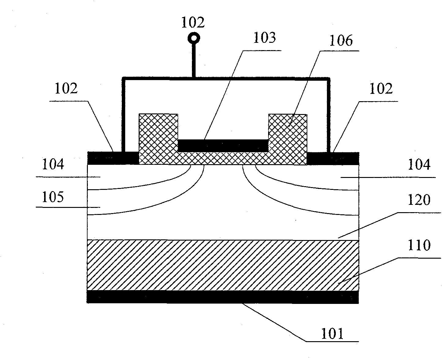
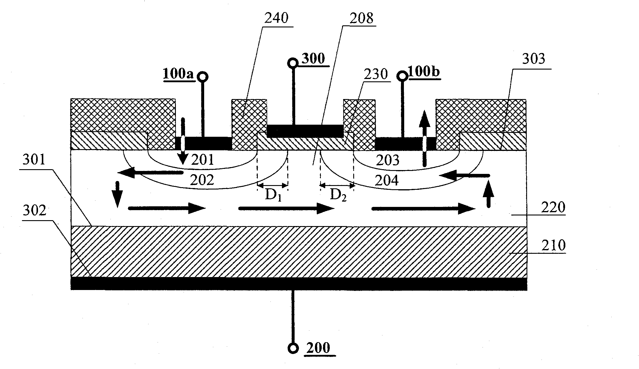
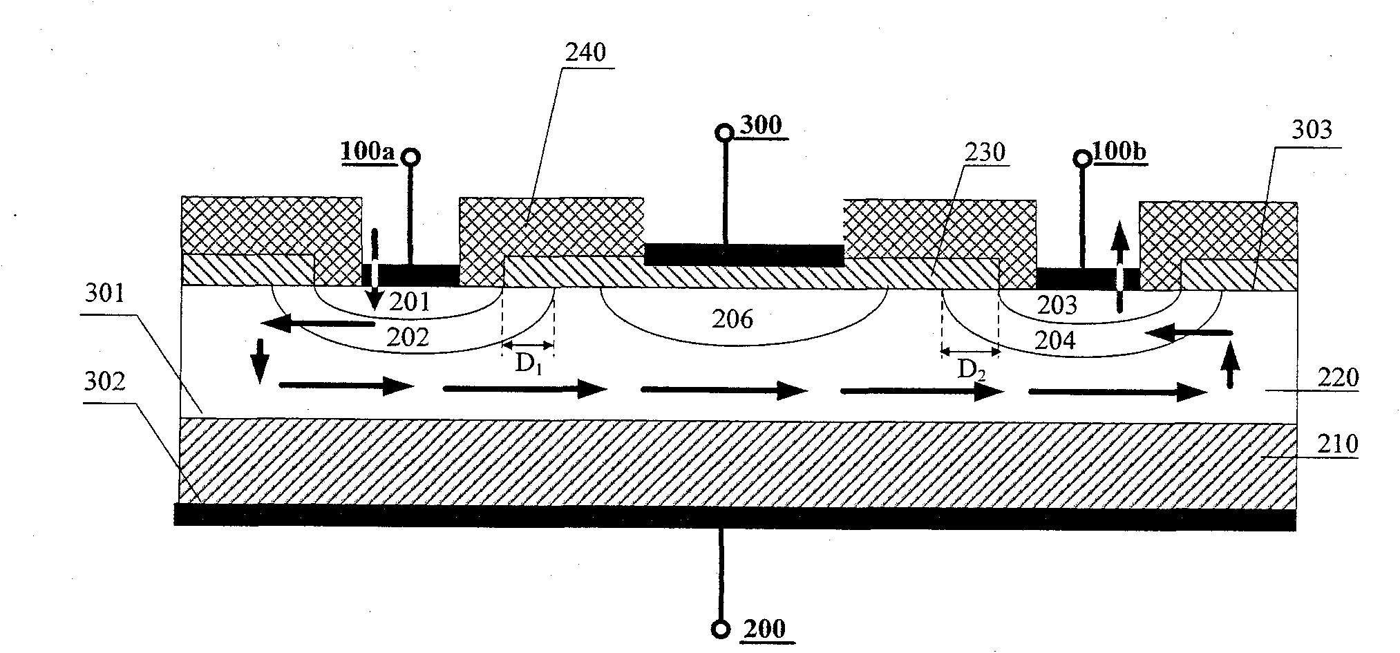
[0033] figure 2 It is a schematic diagram of the first embodiment of the VDMOS transistor test structure provided by the present invention.

[0034] Such as figure 2 As shown, the VDMOS transistor test structure provided in this specific embodiment includes: a semiconductor substrate 210 of the first conductivity type; an epitaxial layer 220 of the first conductivity type located on the upper surface 301 of the semiconductor substrate 210; The non-overlapping first source doping region 201 and the second source doping region 203, wherein both the first source doping region 201 and the second source doping region 203 are doped with the first semiconductor type; located in the first source The first channel region 202 below the doped region 201 and the second ch...


PUM


Abstract

The invention relates to a VDMOS (Vertical Double-diffusing Metal-Oxide-Semiconductor) transistor testing structure which belongs to the technical field of semiconductors and comprises a semiconductor substrate, an epitaxial layer, a first source doping region, a second source doping region, a channel region and an interlevel dielectric layer, a metal layer covering the upper surface of the semiconductor substrate and used for leading out two source electrodes and grid electrodes and a back metal layer covering the bottom surface of the semiconductor substrate, wherein the channel region positioned below the source doping region is mutually separated to form double channels, and the source electrode positioned on the surface of the epitaxial layer is mutually cut off to be respectively used as a test source electrode and a test drain electrode. Under the control of the voltage of the grid electrode, the test is carried out by using the test source electrode and the test drain electrode as output electrodes, the invention effectively realizes that the on resistance of the VDMOS transistor is tested, overcomes the difficulty of superficial characteristics after grinding and unifies the test program, thereby further lowering the maintenance and development cost, and improving the product test and feedback efficiency.

Description

technical field [0001] The invention relates to a test structure of a transistor device, in particular to a test structure suitable for a VDMOS crystal [0002] The invention discloses a test structure of a tube (vertical double-diffused field-effect transistor), belonging to the technical field of semiconductors. Background technique [0003] In a semiconductor integrated circuit, a circuit based on a double-diffused field-effect transistor, referred to as DMOS, uses the difference in the lateral diffusion speed of two impurity atoms to form a self-aligned sub-micron channel, which can achieve a very high operating frequency. and speed. [0004] Compared with ordinary MOS transistors, DMOS has two main differences in structure: one is that P-type and N-type impurities are sequentially diffused through the same oxide layer window to form a very short channel; A lightly doped N - The drift region has a much lower doping concentration than the channel region. This region b...

Claims


Application Information

Patent Timeline
Patent Type & Authority Applications(China)
IPC IPC(8): H01L29/78H01L29/10H01L23/544
Inventor 刘宪周克里丝
Owner SHANGHAI HUAHONG GRACE SEMICON MFG CORP
Why Eureka
Try Eureka