Metal substrate and light-emitting diode encapsulation method of metal substrate

A technology of metal substrate and packaging method, which is applied in the direction of electrical components, electric solid devices, circuits, etc., can solve the problems of low light extraction efficiency, poor heat dissipation, and poor light color performance of white light, so as to reduce production costs and reduce new interfaces. Spawn chance, remove the effect of the air interface

CN101820044AInactive Publication Date: 2010-09-01江苏米优光电科技有限公司
5 Cites 16 Cited by

Patent Information

Authority / Receiving Office
CN · China
Current Assignee / Owner
Publication Date
2010-09-01
Estimated Expiration
Not applicable · inactive patent

Smart Images

  • Figure 1
    Figure 1
  • Figure 2
    Figure 2
  • Figure 3
    Figure 3
Patent Text Reader

Abstract

The invention discloses a metal substrate and a light-emitting diode (LED) encapsulation method of the metal substrate. The encapsulation method comprises the following steps: stamping a lens installation slot, a fluorescent powder coating slot and an electrode pad on the metal substrate, forming an insulating layer on the substrate, adopting the silk screen printing method to form a eutectic solder pad, a reflecting metal layer, a lead and a metal solder pad; then performing eutectic welding of a chip on the metal substrate; adding fluorescent powder, sending the metal substrate in an oven to solidify fluorescent powder; installing a lens, injecting adhesive, sending the metal substrate in the oven for solidifying; and cutting the circuit board to obtain a high power LED encapsulated by the substrate. The invention provides the metal substrate and the LED encapsulation method of the metal substrate; and the encapsulation technology of the metal substrate adopts the stamping technology and the silk screen printing technology so that the accuracy of patterns on the substrate can be ensured and the material cost can be saved.
Need to check novelty before this filing date? Find Prior Art

Description

technical field

[0001] The invention belongs to the technical field of semiconductor manufacturing, and relates to a metal substrate and an LED packaging method of the metal substrate. Background technique

[0002] Power-type light-emitting diodes (Light Emitting Diode, LED) are considered to be the most potential semiconductor devices to replace various existing lighting sources. Currently, there are two types of power packages on the market: stand-off type and substrate type. There are Luxeon series launched by Lumileds Company, Dragon series launched by Osram Company and Xlamp series launched by Cree Company. Many domestic packaging manufacturers imitate their appearance. The advantage of bracket type packaging is that the structure of the device is stable, the process is easy to mass produce, and it is suitable for eutectic soldering, phosphor colloid, and lens molding. However, its outstanding disadvantage is that there are more intermediate heat sinks and heat dissi...

Examples

Embodiment 1

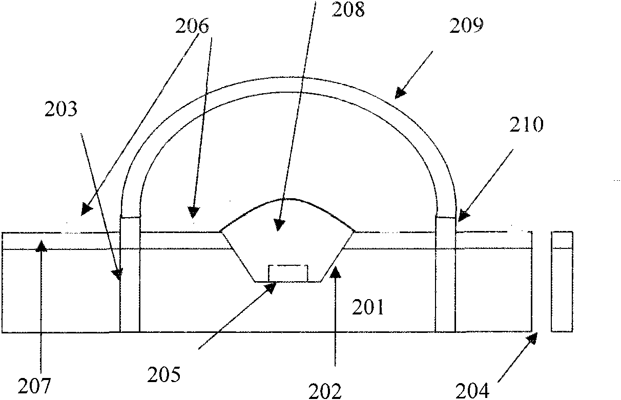
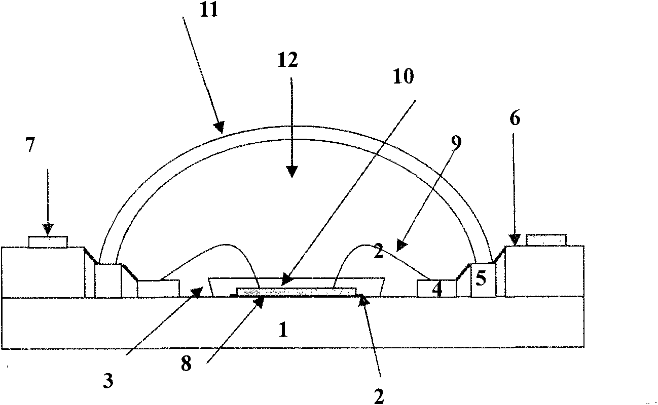
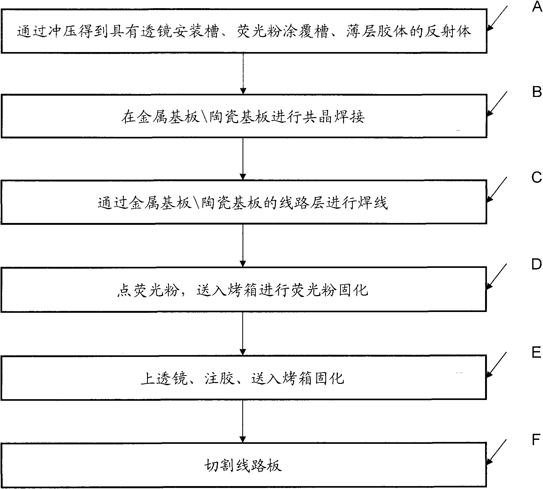
[0041] The invention provides a packaging method of a high-power white light LED based on a metal substrate. Firstly, a metal substrate is designed, by punching out the lens mounting groove, the phosphor coating groove and the electrode pad, and forming an insulating layer on the substrate, and forming a eutectic pad, a reflective metal layer, leads and wires by screen printing. metal pads. Eutectic bonding of the chip is then performed on the metal substrate. Point the phosphor powder and send it to the oven for phosphor curing. Put on the lens, inject glue, and send it to the oven for curing. Cut the circuit board to obtain the high-power LED packaged on the substrate.

[0042] In the present invention, the metal substrate structure is as Figure 4 to Figure 7. For the convenience of description, only one unit is used for illustration; the substrate can use a single-row structure of 1×12 units, or a double-row structure of 2×10 units, or other suitable unit arrangements...