Single-power clock clocked transmission gate ternary heat insulating circuit and T computing circuit

An adiabatic circuit, transmission gate technology, applied in logic circuits, electrical components, pulse technology, etc., can solve problems such as increased wiring complexity and clock energy consumption

Inactive Publication Date: 2010-09-15
NINGBO UNIV
View PDF4 Cites 21 Cited by
  • Summary
  • Abstract
  • Description
  • Claims
  • Application Information

AI Technical Summary

Problems solved by technology

Among them, such as the document "Design of a DTCTGAL Circuit and Its Application" published by Journal of Semiconductors ("Design of a DTCTGAL Circuit and Its Application" based on dual-power clock), author: Wang Pengjun, Li Kunpeng, MeiFengna (Wang Pengjun , Li Kunpeng, Mei Fengna), who proposed a design scheme using dual-power clock technology to realize multi...

Method used


Image

  • Single-power clock clocked transmission gate ternary heat insulating circuit and T computing circuit
  • Single-power clock clocked transmission gate ternary heat insulating circuit and T computing circuit
  • Single-power clock clocked transmission gate ternary heat insulating circuit and T computing circuit

Examples


Embodiment 1

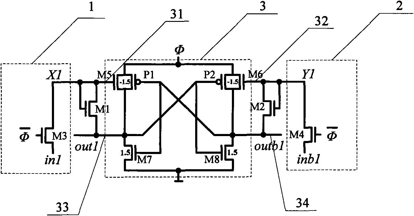
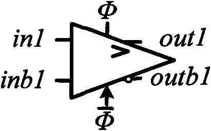
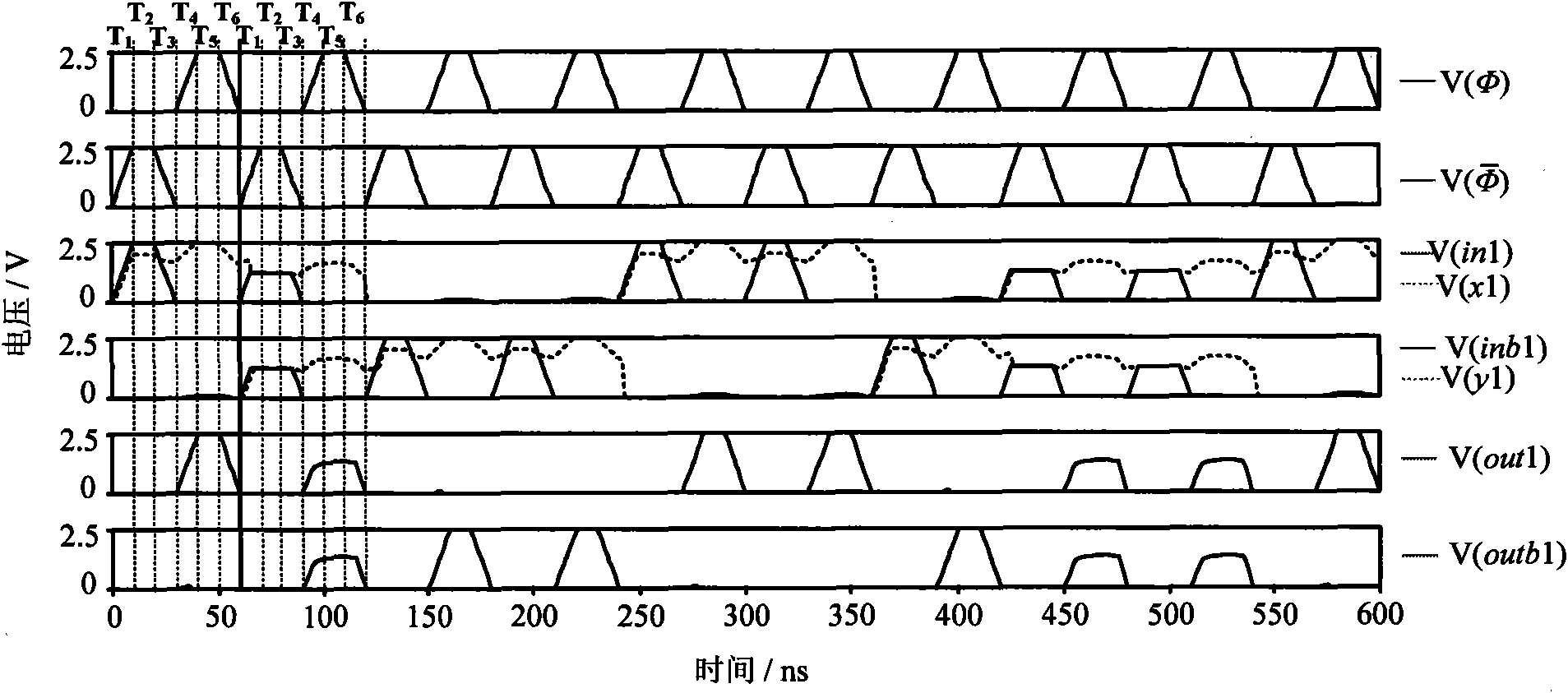
[0031] Based on the research on the adiabatic logic circuit of the binary clock-controlled transmission gate, the present invention proposes a three-valued adiabatic circuit of the single-power clock-controlled transmission gate. The three-valued adiabatic circuit of the transmission gate is divided into two stages of operation: the first stage Level corresponds to the clocked clock signal of logic 2 Under the control, the clocked NMOS transistor is used to complete the sampling of the input signal; the second stage uses the sampled value and the cross storage structure unit to complete the assignment of the output load under the working rhythm of the power clock signal Φ whose amplitude level corresponds to logic 2 And energy recovery, and the output signal and complementary output signal can effectively eliminate the floating. Among them, Φ and The phase difference is 180°, and the amplitudes are all V DD , representing logic 2, in addition to V DD / 2 represents logic 1...

Embodiment 2

[0041] As a multi-valued logical operation operator, T operation constitutes a complete system of multi-valued algebra (T operator algebra), which provides a new way for the research of multi-valued logic theory and application, and can use T operation circuit to construct T operation network to realize Arbitrary multi-valued logic circuit, so the present invention proposes a new T operation circuit clocked by a single power clock.

[0042] A kind of single-power clock clocking T operation circuit proposed by the present invention is as follows: Figure 3a As shown, its symbol is as Figure 3b As shown, it is mainly composed of the transmission gate ternary adiabatic circuit 4 and the ternary adiabatic word operation circuit (comprising the first word operation circuit unit 5 and the second word operation circuit unit 6, respectively as shown in the first embodiment) Figure 4a and Figure 4b shown), the ninth NMOS transistor M9, the tenth NMOS transistor M10, the eleventh N...


PUM


Abstract

The invention discloses a single-power clock clocked transmission gate ternary heat insulating circuit and a T computing circuit. The heat insulating circuit adopts a single-power clock technology to combine the high-information density characteristic of a multi-value logic circuit and the low-power consumption characteristic of a heat insulating circuit and is designed by utilizing a switch-signal algebraic system. The operation of the heat insulating circuit comprises two stages, wherein in the first stage, under the control of a clocked clock, a clocked NMOS (N-Mental-Oxide-Semiconductor) tube is used for sampling an input signal; and in the second stage, under the working rhythm of the single-power clock, a bootstrap-operation NMOS tube and a crossing storage structure are used for charging and discharging a load, and an NMOS tube grid leak parallel connection technology is utilized to ensure that the circuit realizes ternary input and output. The circuit has simpler structure and lower power consumption compared with a gate level circuit. When the working frequency is 16.7MHz, within 1.4 microseconds, the ternary heat insulating can averagely save the energy by about 66.4 percent compared with a DTCTGAL (Double Power Clock Ternary Clocked Transmission Gate Adiabatic Logic) circuit and averagely save the energy by about 85.1 percent compared with a ternary DPL (Double-Pass-Transistor Logic) circuit. The T computing circuit is designed on the basis of the heat insulating circuit, and any ternary logic circuit can be constructed through the T computing circuit.

Description

technical field [0001] The invention relates to a three-value clock-controlled transmission gate adiabatic logic circuit, in particular to a single-power clock-controlled transmission gate three-value adiabatic circuit and a T operation circuit. Background technique [0002] Binary signal (0, 1) is widely used in digital circuits, and it is a signal representation with the least amount of information. In order to enhance the information processing capability of digital systems, the research on multi-valued logic circuits has become an important one of the directions. Due to the increase in the amount of information per wiring and the reduction in the number of input and output leads, the multi-valued logic circuit effectively improves the ability of a single line to carry information and the information density of an integrated circuit, thereby correspondingly increasing the time and space of a multi-valued logic circuit. The utilization rate and effectively reduce the prod...

Claims


Application Information

Patent Timeline
IPC IPC(8): H03K19/017
Inventor 汪鹏君高虹
Owner NINGBO UNIV
Why Eureka
Try Eureka