Nickel-gold electroplating process of PCB

A technology of printed circuit board and nickel-gold electroplating, applied in the direction of secondary processing of printed circuit, etc., can solve the problem of inability to realize nickel-gold electroplating of printed circuit board, etc., and achieve the effects of excellent appearance, high feasibility and cost reduction.

Inactive Publication Date: 2010-09-15
CHINA CIRCUIT TECH SHANTOU CORP
View PDF2 Cites 23 Cited by
  • Summary
  • Abstract
  • Description
  • Claims
  • Application Information

AI Technical Summary

Problems solved by technology

However, if the area to be electroplated with nickel gold is not located at the edge of the surface of the printed circuit board, but is located in the non-edge area of ​​the surface of the printed circuit board (that is, the inner area of ​​the surface of the printed circuit board), due to the area to be electroplated with nickel gold It is located in the non-edge area of ​​the surface of the printed circuit board, so the conventional nickel-gold electroplating process of the printed circuit board cannot design the electroplating leads required for electroplating nickel-gold on the area to be electroplated with nickel-gold. Therefore, the electroplating nickel-gold of the conventional printed circuit board The gold process cannot achieve the electroplating of nickel and gold in the non-edge area of ​​the printed circuit board

Method used


Image

  • Nickel-gold electroplating process of PCB
  • Nickel-gold electroplating process of PCB
  • Nickel-gold electroplating process of PCB

Examples


Embodiment 1

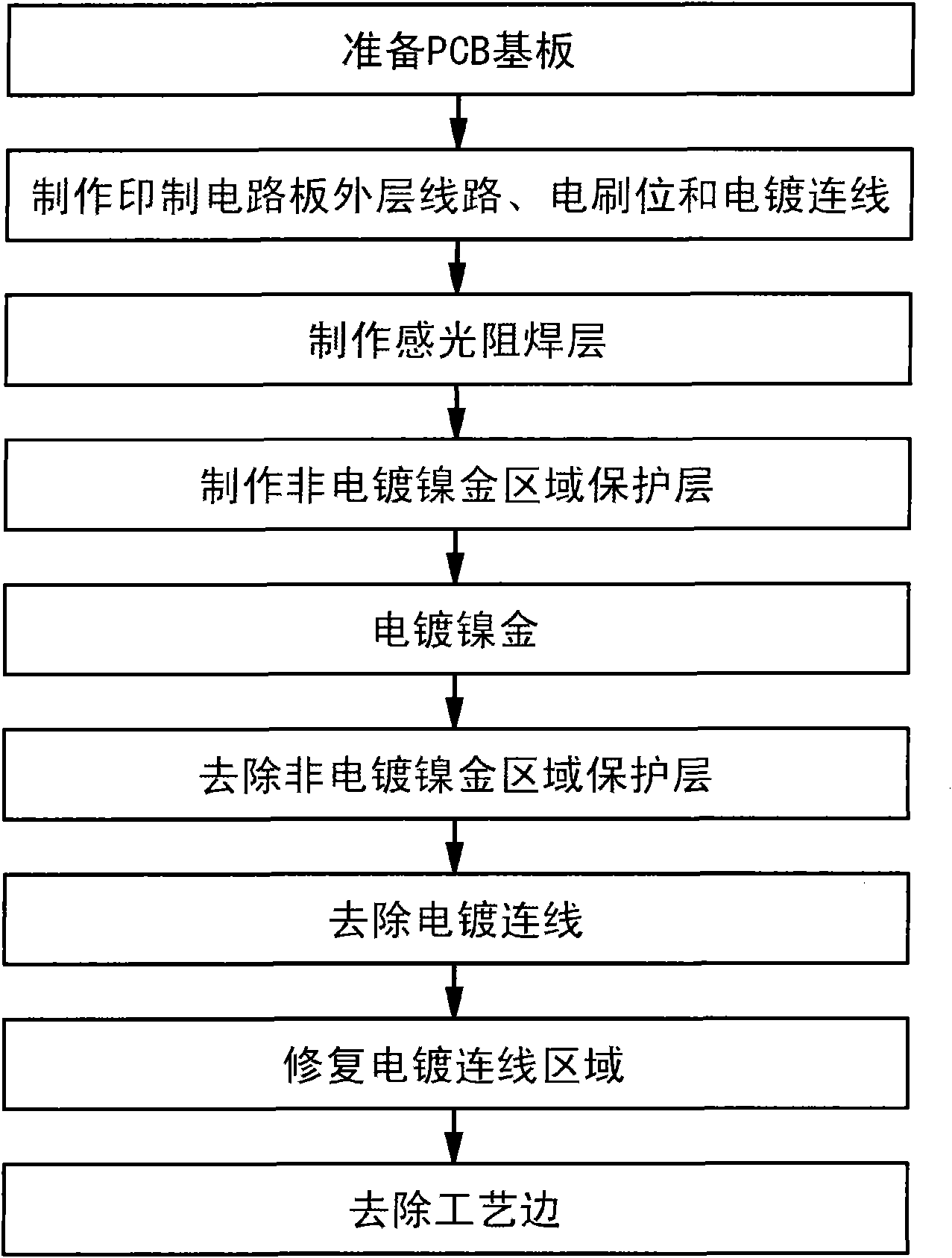
[0034] like Figure 1 to Figure 6 Shown, the nickel-gold electroplating process of printed circuit board in the present preferred embodiment comprises the following steps:

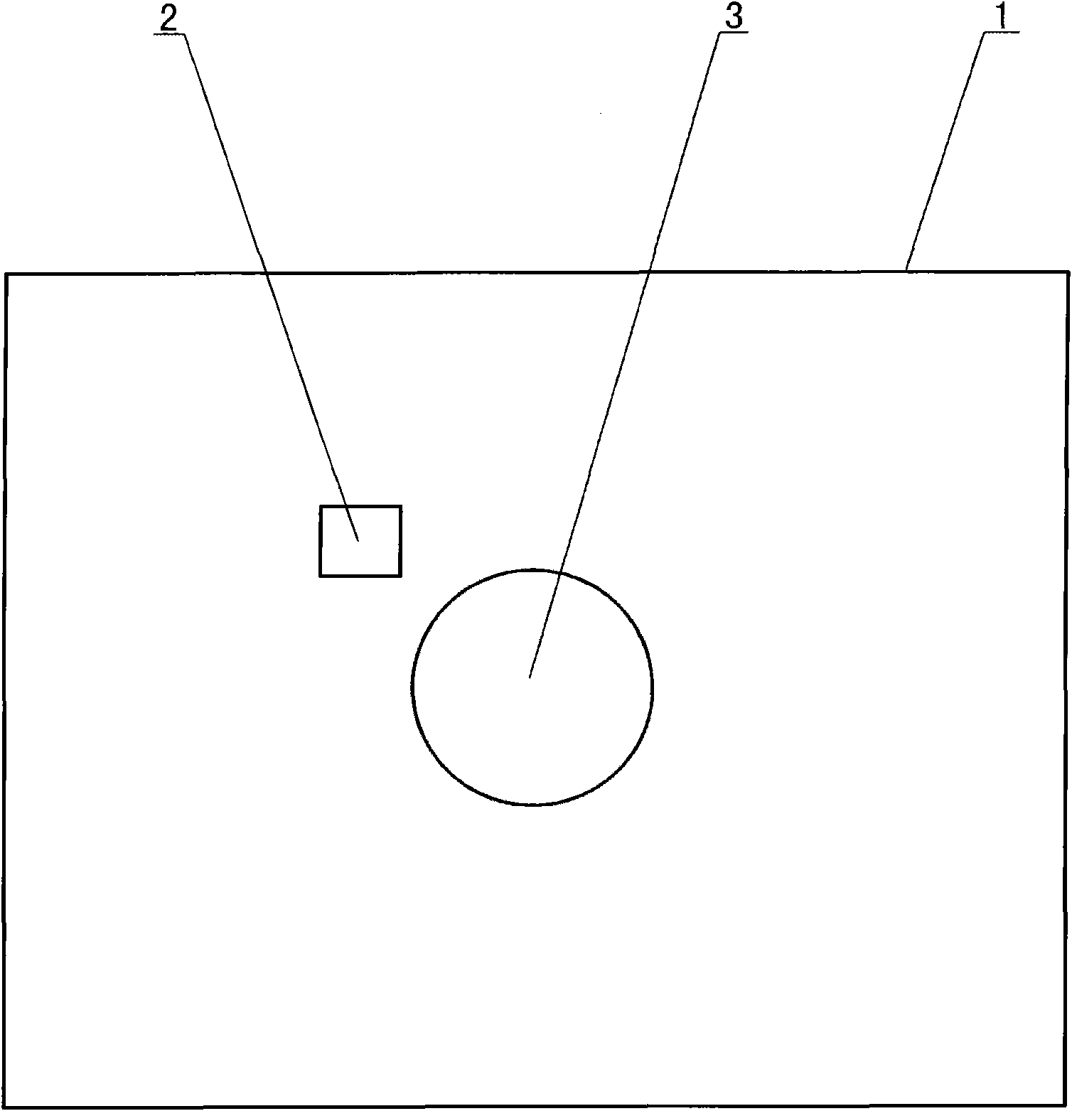
[0035] (1) Prepare PCB substrate 1: as figure 2 As shown, the above-mentioned PCB substrate 1 is a single-layer PCB substrate, and the above-mentioned PCB substrate 1 is provided with a packaging pad 2 and an area 3 to be electroplated with nickel and gold, and the above-mentioned area 3 to be electroplated with nickel and gold is located in the non-edge area of ​​the surface of the PCB substrate 1;

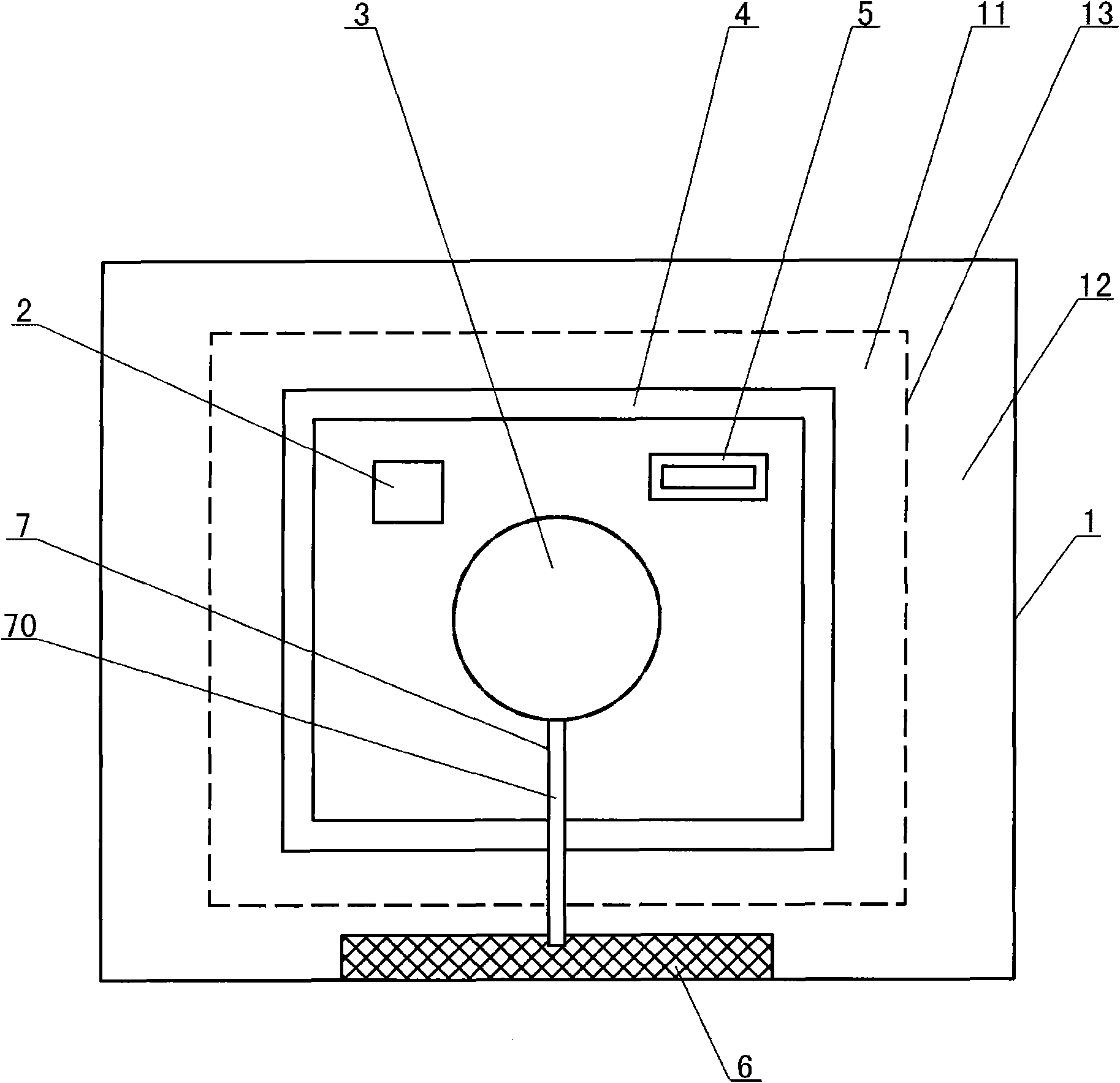
[0036] (2) Make printed circuit board outer circuit 4, 5, brush position 6 and electroplating connection 7: as image 3 As shown, the PCB substrate 1 is divided into a printed circuit board area 11 and a process edge 12, and the boundary line between the printed circuit board area 11 and the process edge 12 is 13; by etching, the printed circuit board area 11 is made. Make circuit board outer layer circuit...

Embodiment 2

[0046] Embodiment 2 is basically the same as Embodiment 1, the difference between the two is:

[0047] like Figure 7 As shown, the PCB substrate 1 in Embodiment 2 is a multilayer PCB substrate. The above-mentioned multilayer PCB substrate, before making the outer layer circuit of the printed circuit board, the brush position and the electroplating connection, completes the internal circuit board according to the conventional printed circuit board process. Layer circuit production, different circuit layer lamination, and then drilling and through the process of electroless copper plating and electroplating copper to realize the conduction of the interlayer circuit; when making the photosensitive solder resist layer, the plug-in mounting hole 10 of the above-mentioned multi-layer PCB substrate belongs to non- In the exposed area, when the exposure is performed, the photosensitive solder resist layer on the plug-in mounting hole 10 is not exposed and is removed by developing.


PUM


Abstract

The invention relates to a nickel-gold electroplating process of a PCB, which comprises the following steps of: (1) preparing a PCB substrate; (2) making an outer circuit, an electric brush part and an electroplating connecting line of the PCB; (3) making a photosensitive soldering-resistant layer; (4) making a non-nickel-gold electroplating region protection layer; (5) electroplating nickel and gold; (6) removing the non-nickel-gold electroplating region protection layer; (7) removing the electroplating connecting line; (8) repairing an electroplating connecting line region; and (9) removing a process edge. In the nickel-gold electroplating process, the electric brush part on the process edge is communicated with a non-marginal to-be-electroplated region by the designed electroplating connecting line to electroplate a non-marginal region on the PCB, the electroplating connecting line is removed after nickel-gold electroplating, and the electroplating connecting line region is repaired to avoid the problem of electroplating connecting line residue and ensure the reliability of the PCB. Meanwhile, the non-marginal to-be-electroplated region and the electroplating connecting line can be freely selected according to actual needs. Accordingly, the nickel-gold electroplating process has high practicability.

Description

technical field [0001] The invention relates to a manufacturing process of a printed circuit board, more specifically, relates to a nickel-gold electroplating process of a printed circuit board. Background technique [0002] Printed circuit board, that is, PCB board, the abbreviation of English (Printed Circuit Board). In order to avoid the oxidation and pollution of printed circuit boards before packaging components, it is necessary to protect the surface of printed circuit boards, that is, surface technology. Commonly used surface processes for printed circuit boards include hot air leveling, electroless nickel-gold, chemical silver, chemical tin, organic protective film, electroplating nickel-gold and other processes. [0003] In the surface technology of printed circuit boards, the nickel-gold plating process is one of the important surface processes. The nickel-gold electroplating process of printed circuit boards uses the principle of an electrolytic cell to use the ...

Claims


Application Information

Patent Timeline
Patent Type & Authority Applications(China)
IPC IPC(8): H05K3/22C25D3/48C25D3/12C25D5/02
Inventor 孟凡义谢若彬郑银周刘明玮黄志东苏维辉杨晓新郑惠芳沈斌苏启能谢少英郑国光刘建生
Owner CHINA CIRCUIT TECH SHANTOU CORP
Why Eureka
Try Eureka