
Touch type liquid crystal display, touch method, array substrate and manufacture method thereof

A technology for liquid crystal displays and array substrates, applied in the fields of touch-type liquid crystal displays, array substrates and their manufacture, and touch methods, capable of solving the problems of increasing liquid crystal panels, floating images, increasing manufacturing processes and production costs, etc.

Inactive Publication Date: 2010-09-22
BOE TECH GRP CO LTD +1
View PDF0 Cites 16 Cited by
  • Summary
  • Abstract
  • Description
  • Claims
  • Application Information

AI Technical Summary

Problems solved by technology

Practical use shows that the liquid crystal display with the touch panel attached to the liquid crystal panel in the prior art has the following technical defects: (1) the attached touch panel will increase the thickness of the liquid crystal panel, and due to the need to increase the additional cost of attaching the two panels to each other (2) Since the touch panel is attached to the liquid crystal panel, the transmittance of the liquid crystal panel decreases, and the resulting light parallax causes the image to float excessively, thereby affecting the quality of the picture; (3) ) The exposed touch panel will be affected by the external environment and reduce the life
[0004] In addition, in order to realize the touch function of the existing liquid crystal display, the pixel voltage of the front pixel area on the array substrate can be obtained in real time, and the pixel voltage can be used as a reference voltage to compare with the change of the charging voltage obtained when a touch event occurs. Realize the judgment of the touch event; however, the pixel voltage used as the reference voltage in this scheme is different at every moment, and using the pixel voltage as the reference voltage to realize the judgment of the touch event will make the signal processing process complicated and error-prone, and The manufacturing process of liquid crystal display is complex and other defects

Method used


Image

  • Touch type liquid crystal display, touch method, array substrate and manufacture method thereof
  • Touch type liquid crystal display, touch method, array substrate and manufacture method thereof
  • Touch type liquid crystal display, touch method, array substrate and manufacture method thereof

Examples


Embodiment Construction

[0067] The technical solutions of the present invention will be described in further detail below with reference to the accompanying drawings and embodiments.

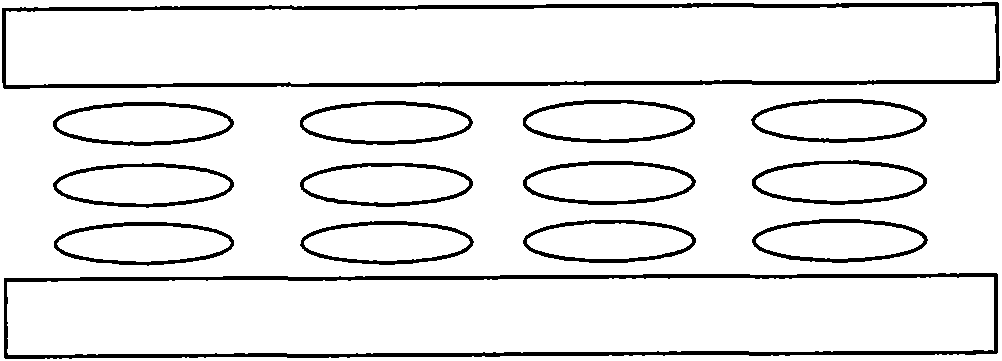
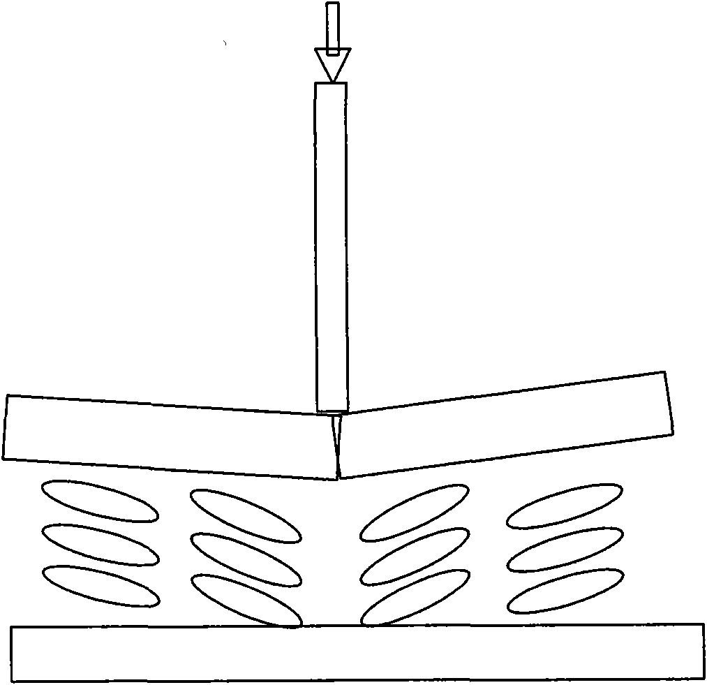
[0068] figure 1 Shown is a schematic diagram of liquid crystal arrangement when the liquid crystal panel of the present invention is not touched, figure 2 Shown is a schematic diagram of liquid crystal arrangement when the liquid crystal panel of the present invention is touched, as figure 1 and figure 2 As shown, the liquid crystal material is filled between the pixel electrode and the common electrode. When the liquid crystal panel is touched, the gap between the liquid crystal cells will change, and then the orientation of the liquid crystal will change. Because the liquid crystal has anisotropic characteristics, that is, its vertical dielectric The electrical constant and the horizontal dielectric constant are different from each other, so the change of the orientation of the liquid crystal will cause the chang...


PUM


Abstract

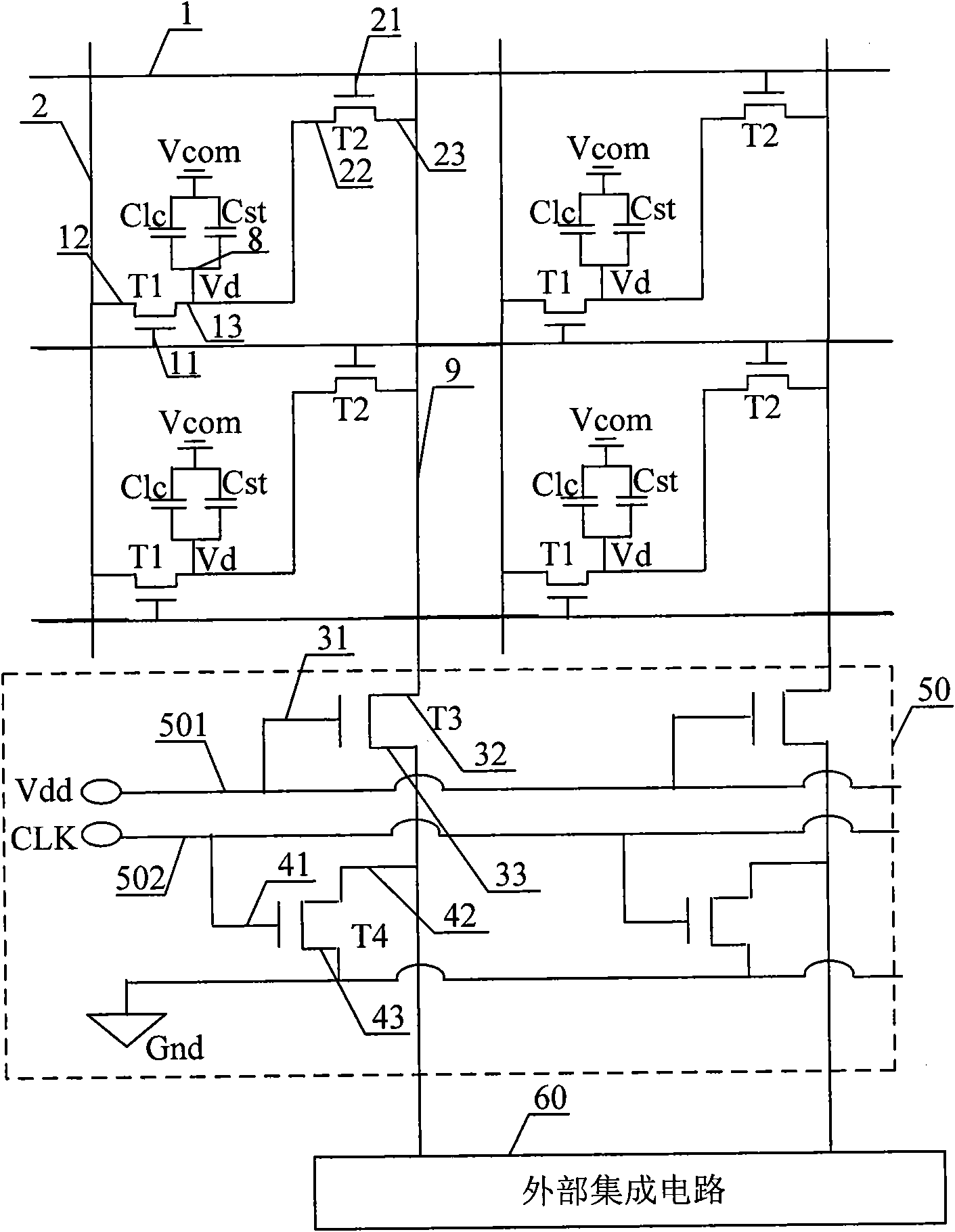
The invention discloses a touch type liquid crystal display, a touch method, an array substrate and a manufacture method thereof, wherein the touch type liquid crystal display comprises a color film substrate, the array substrate and a liquid crystal molecule layer arranged between the color film substrate and the array substrate; a grid line and a data line are formed on the array substrate; and a pixel electrode and a first thin film transistor are formed in a pixel region limited by the grid line and the data line. The array substrate also comprises a second thin film transistor, a signal line, a voltage acquisition circuit and an external integrated circuit, wherein the second thin film transistor is connected with the first thin film transistor and used for acquiring data voltage and black frame voltage of the current pixel region at intervals; the signal line is connected with the second thin film transistor and used for outputting the data voltage and the black frame voltage, and the signal line is arranged parallel to the data line; the voltage acquisition circuit is connected with the signal line and used for acquiring the black frame voltage from the signal line; and the external integrated circuit is used for acquiring the black frame voltage from the voltage acquisition circuit and acquiring a touch position according to the change of the black frame voltage.

Description

technical field [0001] The invention relates to a liquid crystal display, an array substrate and a manufacturing method thereof, in particular to a touch-type liquid crystal display, a touch method, an array substrate and a manufacturing method thereof. Background technique [0002] Liquid Crystal Display (LCD) has the characteristics of small size, low power consumption, and no radiation, and has now occupied a dominant position in the field of flat panel display. The main structure of the liquid crystal display includes an array substrate and a color filter substrate that are boxed together and the liquid crystal material is sandwiched between them. On the array substrate, gate lines that provide scanning signals, data lines that provide data signals, and pixel electrodes that form pixel points are formed. . The working principle of a liquid crystal display to display images is to obtain a desired image signal by applying an electric field to the liquid crystal material a...

Claims


Application Information

Patent Timeline
Patent Type & Authority Applications(China)
IPC IPC(8): G02F1/133G02F1/1362G09G3/36G06F3/041
Inventor 王峥
Owner BOE TECH GRP CO LTD
Learn More