OLED (Organic Light Emitting Diode) lighting substrate, OLED lighting device and manufacturing methods thereof

A technology for lighting devices and manufacturing methods, applied in semiconductor/solid-state device manufacturing, electric solid-state devices, semiconductor devices, etc., can solve problems such as cathode-anode short-circuit light emission, high current intensity, and electrode burnout, so as to reduce the concentration of current intensity, Increase resistance, reduce the effect of easy short circuit

Inactive Publication Date: 2010-09-22
TRULY SEMICON
View PDF3 Cites 8 Cited by
  • Summary
  • Abstract
  • Description
  • Claims
  • Application Information

AI Technical Summary

Problems solved by technology

Although this method is simple, due to the current gathering effect on the anode, the anode in the prior art will make the current intensity generated during the current gathering very large, w

Method used


Image

  • OLED (Organic Light Emitting Diode) lighting substrate, OLED lighting device and manufacturing methods thereof
  • OLED (Organic Light Emitting Diode) lighting substrate, OLED lighting device and manufacturing methods thereof
  • OLED (Organic Light Emitting Diode) lighting substrate, OLED lighting device and manufacturing methods thereof

Examples


Embodiment 1

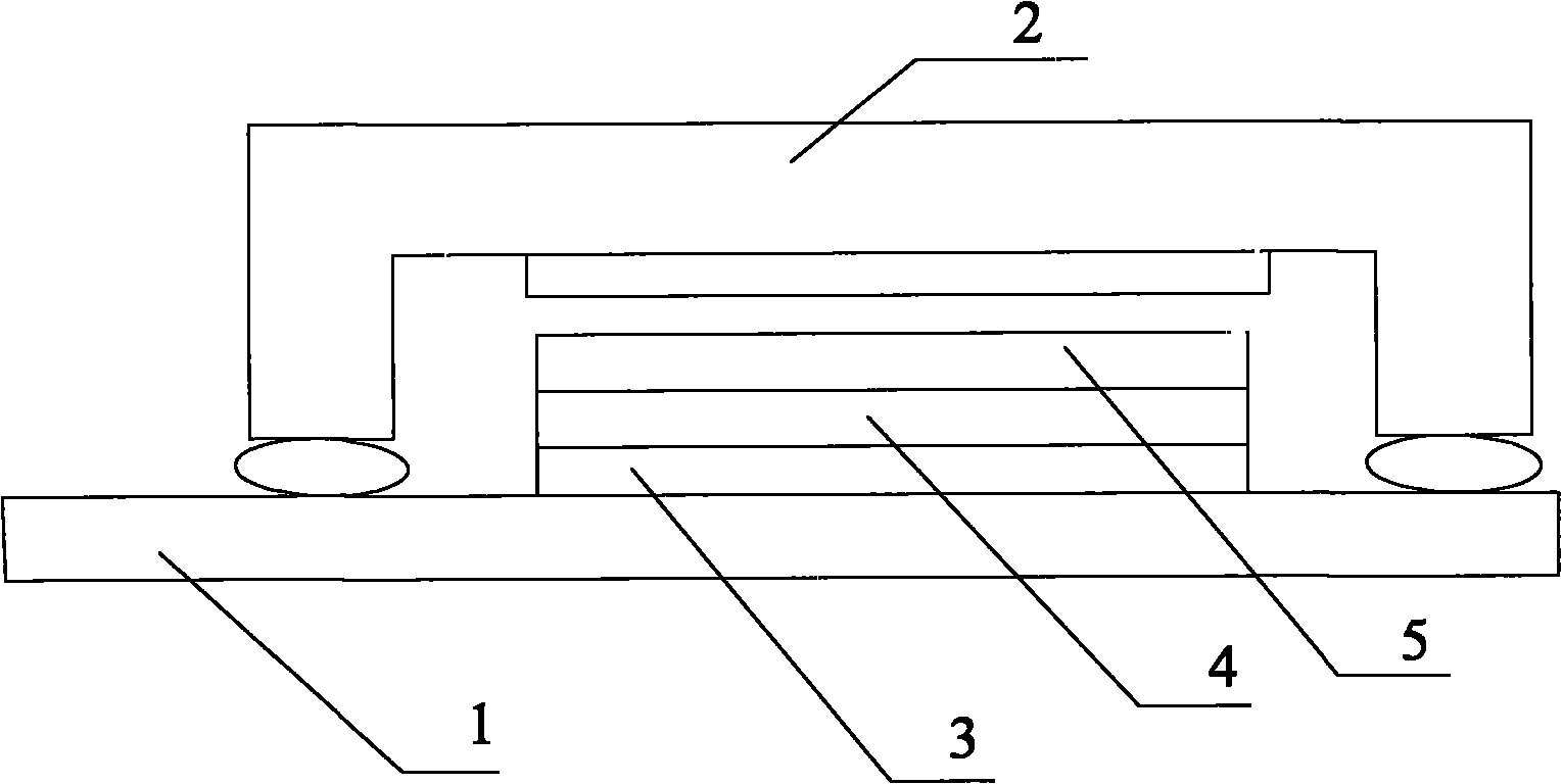
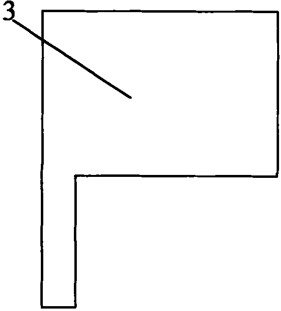
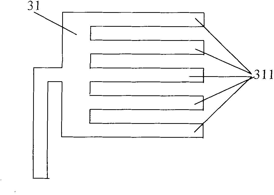
[0052] The substrate includes an anode, an organic functional layer and a cathode arranged in layers, and the anode is a transparent anode, wherein the anode is split into at least two branch anodes. Such as image 3 As shown, it is a schematic diagram of the structure of the substrate anode in this embodiment. The anode 31 includes five branch anodes 311 arranged in parallel. The overall design of the anode in the prior art, in this embodiment, the branch current on each branch anode 311 is about 1 / 5 of the original current, even if a current aggregation effect occurs on a branch anode 311, the accumulated current intensity is greatly weakened .

[0053] By subdividing the anode 31 of the substrate into a plurality of branch anodes, the resistance on each branch anode is increased, so that the branch anodes play a role of shunting, and even if current aggregation occurs on the branch anodes, the concentration of the generated current intensity will be greatly weakened, there...

Embodiment 2

[0056] The substrate includes a stacked anode, an organic functional layer and a cathode, and the anode is a transparent anode. In this embodiment, the substrate anode 41 includes three branch anodes 411 arranged in parallel, such as Figure 4a As shown, it is a schematic cross-sectional view of the substrate anode in this embodiment, and the anode 41 is formed in a comb shape as a whole.

[0057] Since the resistance of each branch anode 411 is relatively large, it will increase loss and generate heat easily. In this embodiment, in order to adjust the resistance of the branch anode 411, in this embodiment, in the direction of each branch anode 411, the organic function The surface of the layer is also covered with an auxiliary electrode layer 412, which is used to reduce the resistance on the branch anode 411. Since the auxiliary electrode layer 412 is opaque, in order not to affect the light-emitting area too much, the line width of the auxiliary electrode layer 412 is small...


PUM

PropertyMeasurementUnit
Line widthaaaaaaaaaa
Thicknessaaaaaaaaaa
Thicknessaaaaaaaaaa

Abstract

Embodiments of the invention provide an OLED (Organic Light Emitting Diode) lighting substrate, an OLED lighting device and manufacturing methods thereof. The OLED lighting substrate comprises an anode, an organic functional layer and a cathode which are laminated, wherein the anode comprises at least two branched anodes for shunting current on the anode. In the embodiments of the invention, the anode formed integrally in the prior art is replaced with the at least two branched anodes, thereby an electrode can be thinned, resistance on each of the branched anodes can be increased, and the branched anode can serve for shunting. Even if current gathering takes place, the intensity of concentrated current produced on the branched anode can also be weakened greatly, current gathering effect can be weakened, and the problems that the cathode and the anode can easily suffer from short-circuit, the electrode can be easily burned and light cannot be uniformly emitted can be solved.

Description

technical field [0001] The invention relates to the technical field of semiconductors, in particular to an OLED lighting substrate, an OLED lighting device and a manufacturing method thereof. Background technique [0002] Organic Light-Emitting Diode (OLED) lighting has many advantages such as low energy consumption, planarization, and large area, and is a booming next-generation lighting technology. [0003] The structure of the OLED lighting device is as figure 1 As shown, it includes: a substrate 1 and a back cover 2 , where an anode 3 , a very thin multi-layer organic functional layer 4 on the anode 3 , and a cathode 5 on the organic functional layer 4 are deposited on the substrate 1 . The principle of OLED light emission is to apply direct current between the cathode 5 and the anode 3 to drive the organic functional layer 4 to emit light. [0004] In the prior art, the fabrication of the anode 3 on the substrate 1 is relatively simple, such as figure 2 As shown, th...

Claims


Application Information

Patent Timeline
IPC IPC(8): H01L51/50H01L51/52H01L51/56
CPCH10K50/813H10K50/814
Inventor 曹绪文何基强
Owner TRULY SEMICON
Why Eureka
Try Eureka