Parallel photoetching write-through system

A lithography direct writing and optical system technology, applied in the field of micro-nano processing devices, can solve the problems affecting the quality of lithography workpieces, defocusing, etc., and achieve high resolution and improve efficiency.

Active Publication Date: 2010-09-29
SVG TECH GRP CO LTD +1
View PDF1 Cites 45 Cited by
  • Summary
  • Abstract
  • Description
  • Claims
  • Application Information

AI Technical Summary

Problems solved by technology

However, generally speaking, the fluctuation of the workpiece surface is above 10 microns, while the focal depth of the high-resolution optical system is below 1 micron, and there are also fluctuations when the workpiece table is operated in two dimensions. , defocusing phenomenon will occur, thus affecting the quality of photolithographic workpieces

Method used


Image

  • Parallel photoetching write-through system
  • Parallel photoetching write-through system
  • Parallel photoetching write-through system

Examples


Embodiment 1

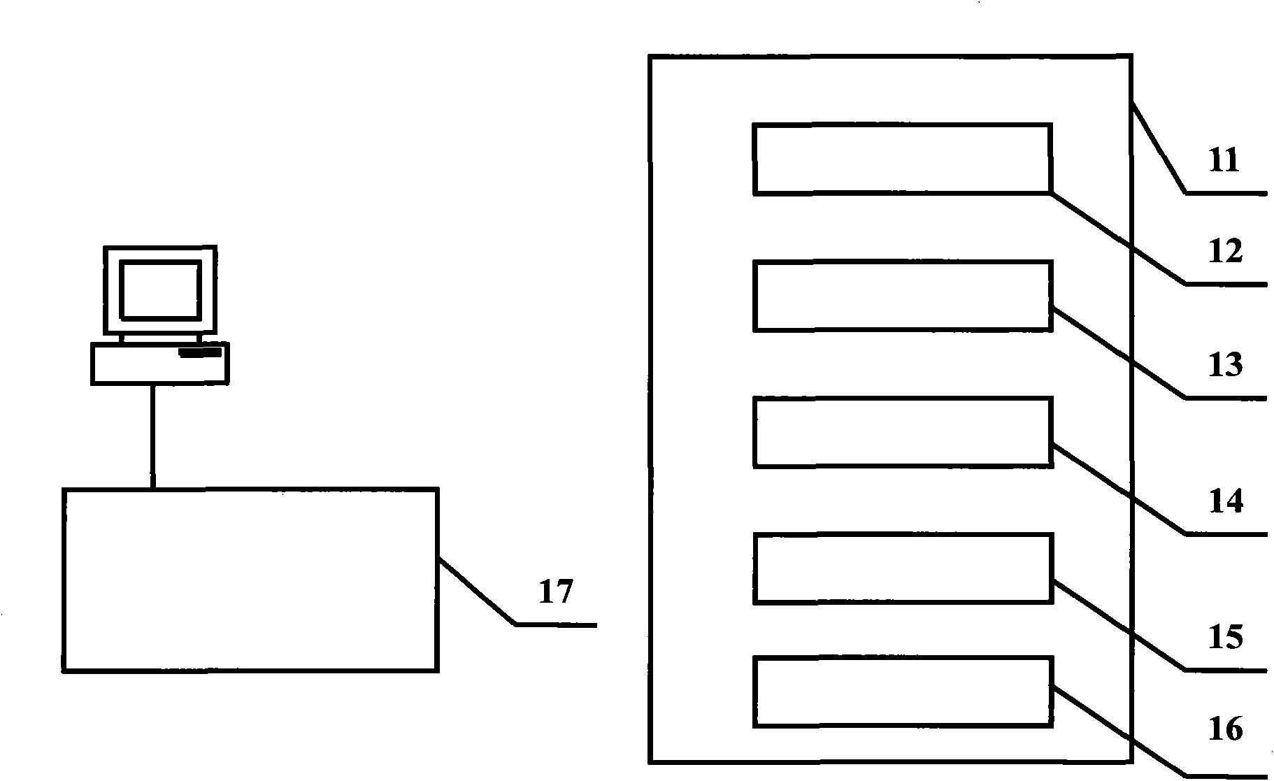
[0032] A multi-axis parallel lithography direct writing system, see Figure 4 As shown, the mechanical frame 41 includes a light source, an optical system, a spatial light modulator, a motion system, and a sensor, and a control computer 417 and a control drive unit 418 are located outside the mechanical frame. The specific description is as follows:

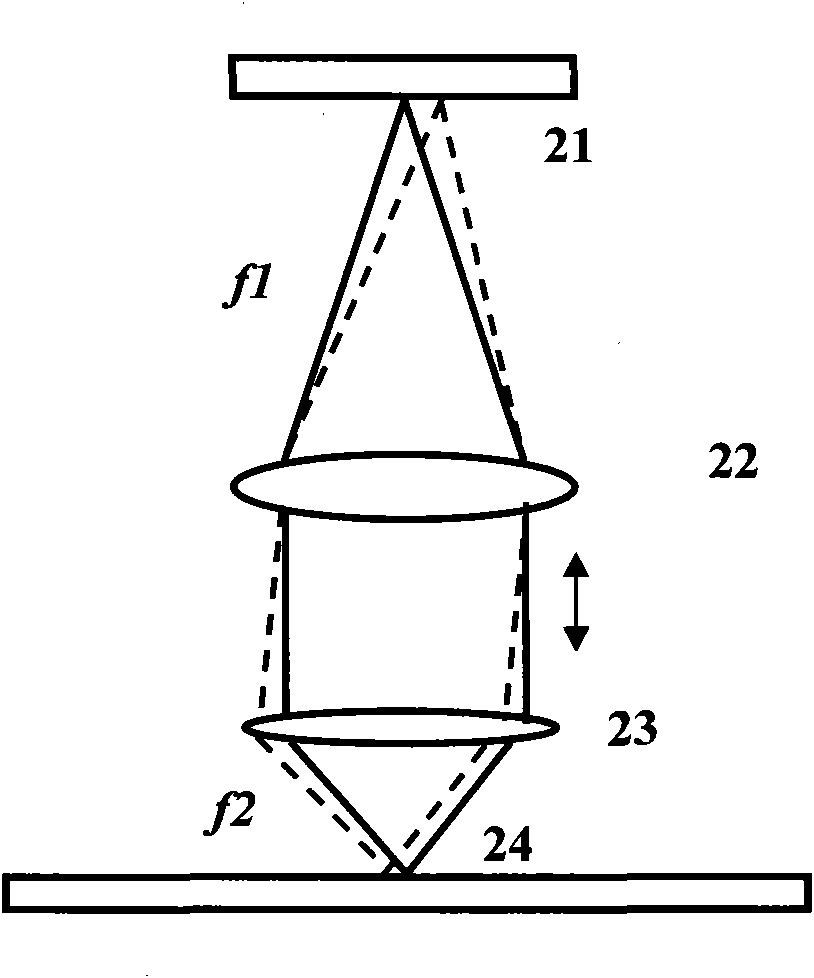
[0033] a) The light emitted by the light source 42 illuminates the spatial light modulator 43 after beam expansion and collimation, the light modulated by the spatial light modulator passes through the partial reflector 44, enters the tube lens (Tube lens) 45, and passes through the partial reflection After the mirror 46 passes through the objective lens 47, the image is placed on the work surface of the workpiece table located on the multi-axis platform 48, and the light reflected from the workpiece surface enters the optical system again, passes through 47, 46, 45, 44, and lens group 49 successively, and enters the CCD sensor 4...

Embodiment 2

[0044] like Figure 5 As shown, the number of motion axes of the motion platform 58 is increased or decreased, and other configurations are the same as in Embodiment 1.

[0045] Reduce the number of motion axes. For example, the X, Y plane direct writing system can be composed of X, Y motion platforms and small-stroke servo moving parts. Similarly, the X, R plane polar coordinate direct writing system can be formed. X, Y, Z systems wait.

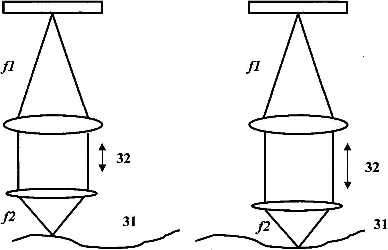
[0046] Increasing the number of motion axes brings more degrees of freedom, enabling the direct writing system to achieve more operating modes. For example, adding an axis that makes the table move in pitch, so that the light is always perpendicular to the workpiece when processing curved surfaces, which improves the processing accuracy.

Embodiment 3

[0048] like Figure 6 As shown, the gantry structure system. The configuration of the optical components remains unchanged. The light source, spatial light modulator, optical system, CCD and Z-axis are taken as a whole. The platform is used to place photolithographic workpieces to form a X, Y, Z gantry three-axis parallel photolithography system. This structure is suitable for designing models with a large photolithography format (greater than 500mm).


PUM

PropertyMeasurementUnit
wavelengthaaaaaaaaaa

Abstract

The invention discloses a parallel photoetching write-through system which comprises a light source, a pattern generating system, an optical system, a control system, a moving system and a workpiece platform. The parallel photoetching write-through system is characterized by also being provided with a focusing servo system, the focusing servo system comprises a detection light path, a sensor and a focusing device, the optical system comprises a micro-system and a detection light path, wherein the micro-system adopts a double axifugal optical system, the detection light path comprises a detection light source, a first light splitter arranged in the double axifugal optical system and a second light splitter arranged between the detection light source and the first light splitter; detection light enters the double axifugal optical system through the first light splitter and irradiates on a workpiece of the workpiece platform; reflective light is received by the sensor through the first light splitter and the second light splitter; and the control system controls the action of the focusing device according to signals of the sensor to realize servo focusing. The invention can realize accurate photoetching of a submicron micro-structure by combining with a focusing imaging servo system.

Description

technical field [0001] The invention relates to a micro-nano processing device, in particular to a photolithographic direct writing system with multiple coordinate axes, which is applied to the research and manufacture of precision mask photolithography, MEMS devices, 3D photolithography, diffractive optics, micro-optics, etc. field. Background technique [0002] The development of industrial technology is inseparable from micro-nano processing technology. Microelectronics technology is a symbol of new technology revolution. In the past few decades, the development of micro-nano processing technology has promoted the leapfrog progress of integrated circuits. At present, micro-nano processing Technology is not only playing an important role in the field of microelectronics, but also promoting the development of new devices and new disciplines, such as micro-electromechanical systems (MEMS), optical integration technology, micro-optics, etc. [0003] Micro-nano-fabrication is...

Claims


Application Information

Patent Timeline
Patent Type & Authority Applications(China)
IPC IPC(8): G03F7/207G03F7/20
Inventor 浦东林胡进朱鹏飞魏国军陈林森
Owner SVG TECH GRP CO LTD
Why Eureka
Try Eureka