Supercharge Your Innovation With Domain-Expert AI Agents!

Mounting processing operation device, operation method and display substrate module assembly line

A technology for operating devices and substrates, applied in nonlinear optics, optics, instruments, etc., can solve problems such as difficulty in improving the accuracy of substrate flatness, and achieve high yield or high operating efficiency

Inactive Publication Date: 2012-06-27
HITACHI HIGH-TECH CORP
View PDF3 Cites 0 Cited by
  • Summary
  • Abstract
  • Description
  • Claims
  • Application Information

AI Technical Summary

Problems solved by technology

[0011] In addition, the conventional adsorption pad disclosed in Patent Document 3 has a structure in which the surface of the panel is directly supported by the adsorption surface, and it is difficult to improve the accuracy of the flatness of the substrate.

Method used


Image

  • Mounting processing operation device, operation method and display substrate module assembly line
  • Mounting processing operation device, operation method and display substrate module assembly line
  • Mounting processing operation device, operation method and display substrate module assembly line

Examples


Embodiment Construction

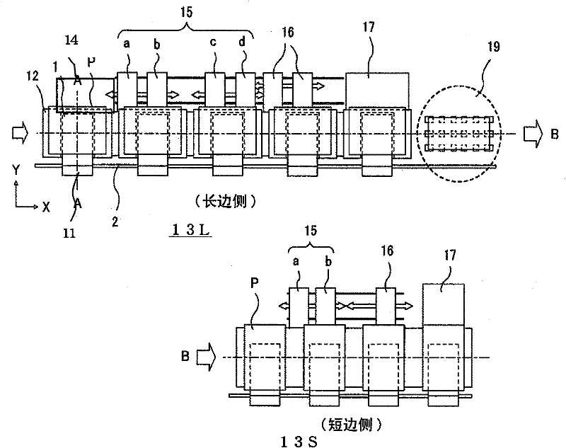
[0058] Below, use Figure 1 to Figure 11 One embodiment of the present invention will be described.

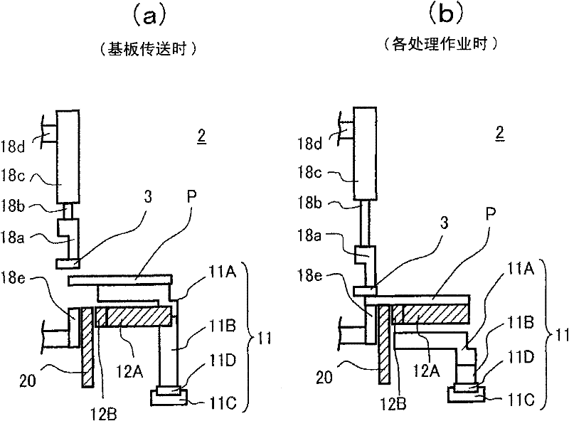
[0059] figure 1 is a diagram showing a display substrate module assembly line 1 according to an embodiment of the present invention, figure 2 It is a figure which shows the basic structure of the transfer apparatus 2 of this board|substrate.

[0060] figure 1 The device is a production line device that transfers substrates sequentially from left to right in the figure through a transfer device, and at the same time performs various processing operations on the peripheral parts of the substrates, and performs mounting and assembly operations such as ICs or TABs. The transfer device includes holding substrates P has a substrate holding mechanism 12 and a transfer arm 11 for transferring the substrate to an adjacent position where a processing device is installed. figure 1 The device of the above-mentioned device first performs the processing on the long side of the substrat...


PUM

PropertyMeasurementUnit
surface smoothnessaaaaaaaaaa

Abstract

The present invention provides an operation edge fixing base which can prevent component loading position precision or jointing reliability reduction caused by display substrate warpage in component loading joint processing of display device, a mounting processing operation device with an operation edge fixing base or a mounting processing operation method using the operation edge fixing base, a production line structure with the mounting operation device or operation method for providing a display substrate module assembly line with high yield rate and high operation efficiency. The mountingprocessing operation device or operation method for mounting components at the periphery of the display substrate comprises the following components: the operation edge fixing base for supporting andloading the operation edge of the loading component from the lower part; two movable side holding parts which support two edges for clamping the operation edge from the lower part; and a conveying moving base with a dimension which allows entering a dent-shaped part that is composed of the operation edge fixing base and the two side holding parts, wherein the operation edge fixing base is also provided with a substrate adsorption pad which adsorbs a planar display substrate after the adsorption of the planar display substrate.

Description

technical field [0001] The present invention relates to so-called TAB (Tape Automated Bonding) connection and mounting of drive ICs on the periphery of FPD (Flat Panel Display) display substrates such as liquid crystal and plasma, or COF (Chip on Film), FPC (Flexible Printed Circuit) and mounting peripherals Substrate (PCB, Printed Circuit Board) installation and processing equipment and display substrate module assembly line composed of them. More specifically, for example, it relates to a mounting processing device and a mounting processing method having a fixed working side base, which is suitable for mounting Processing job of TAB or IC. Background technique [0002] The display substrate module assembly line is to sequentially perform multiple processing operations on the display substrates of FPDs such as liquid crystal and plasma (hereinafter, basically referred to as substrates, and other substrates, such as PCBs, are clearly marked as PCB substrates). Devices such...

Claims


Application Information

Patent Timeline
Patent Type & Authority Patents(China)
IPC IPC(8): G02F1/1333H01J9/20
Inventor 山崎不二夫宫坂彻玉本淳一渡边丰大录范行
Owner HITACHI HIGH-TECH CORP
Features
  • R&D
  • Intellectual Property
  • Life Sciences
  • Materials
  • Tech Scout
  • Unparalleled Data Quality
  • Higher Quality Content
  • 60% Fewer Hallucinations
Learn More