Liquid crystal display panel and manufacture method thereof
A technology for liquid crystal display panels and manufacturing methods, applied to static indicators, instruments, nonlinear optics, etc., can solve the problems of high cost, complicated process, complex structure of liquid crystal display panels, etc., to simplify the structure, simplify the process, save The effect of making steps
- Summary
- Abstract
- Description
- Claims
- Application Information
AI Technical Summary
Problems solved by technology
Method used
Image
Examples
Embodiment 1
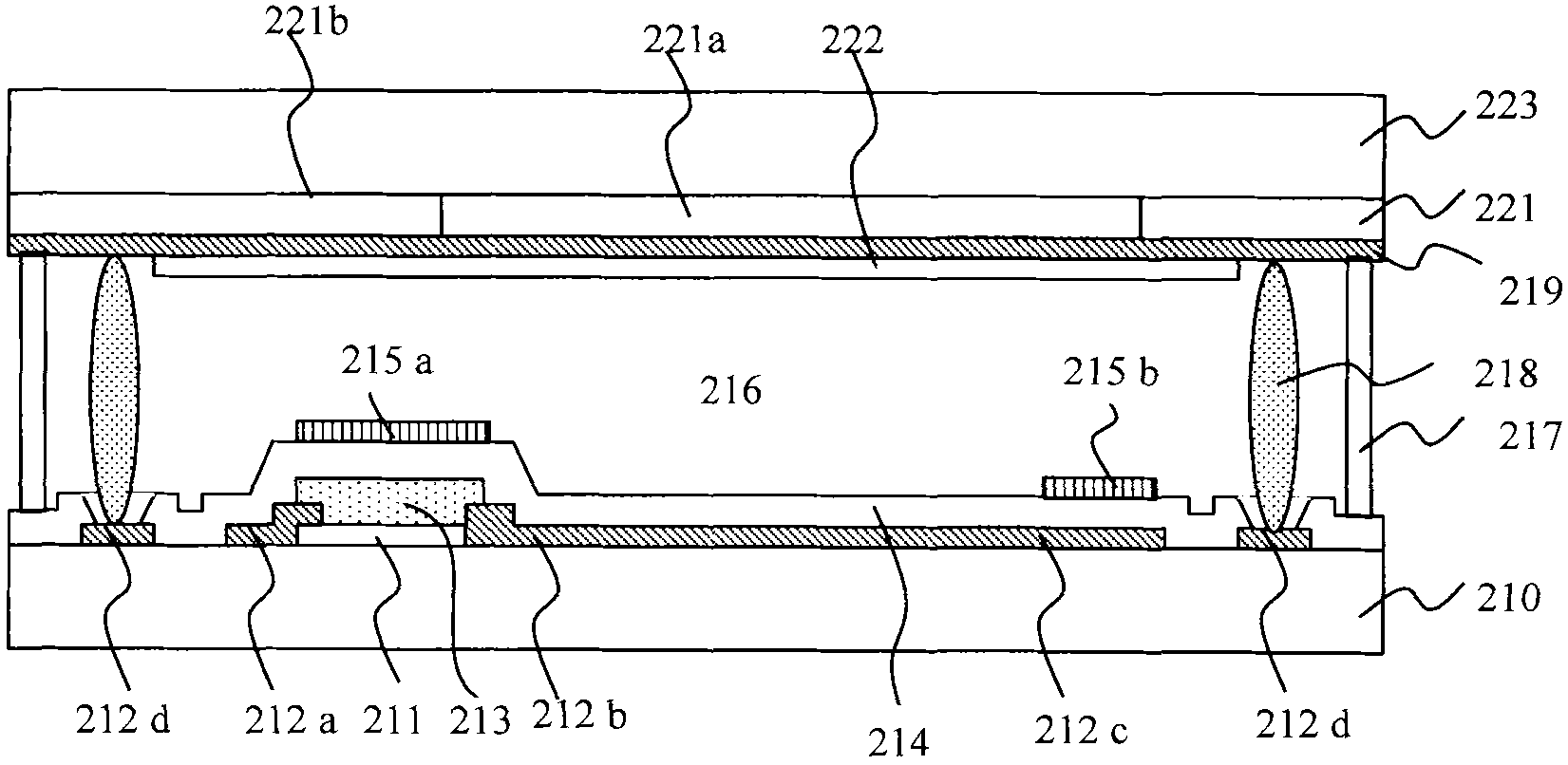
[0067] figure 2 It is a schematic structural diagram of the liquid crystal display panel of the first embodiment of the present invention, combined with figure 2 The structure of the liquid crystal display panel of the first embodiment of the present invention will be described.
[0068] Such as figure 2 As shown, in this embodiment, the liquid crystal display panel includes a first substrate 210 and a second substrate 223 oppositely disposed, and a liquid crystal layer 216 between the first substrate 210 and the second substrate 223 .
[0069] Specifically, the first substrate 210 and the second substrate 223 may be made of transparent glass material or transparent plastic material. On the side facing the second substrate 223, the first substrate 210 has: a light-shielding layer 211, a semiconductor material layer 213 on the light-shielding layer 211, and the first substrate 210 on both sides of the semiconductor material layer 213 has layers covering both sides of the s...
Embodiment 2
[0090] Figure 8 It is a schematic structural diagram of a liquid crystal display panel according to the second embodiment of the present invention, combined below Figure 8 The structure of the liquid crystal display panel of the second embodiment of the present invention will be described.
[0091] Such as Figure 8 As shown, in this embodiment, the liquid crystal display panel includes a first substrate 310 and a second substrate 320 disposed opposite to each other, and a liquid crystal layer 319 located between the first substrate 310 and the second substrate 320 .
[0092] Specifically, the first substrate 310 has a color filter layer 311 on the side facing the second substrate 320, and the color filter layer 311 includes a pigment layer 311a and a black matrix layer (BM) 311b located at the interval between the pigment layers 311a. The upper layer of the black matrix layer (BM) 311b has a semiconductor material layer 314, and the positions on both sides of the semicond...
Embodiment 3
[0113] Figure 10 It is a structural schematic diagram of the liquid crystal display panel of the third embodiment of the present invention, combined with the following Figure 10The structure of the liquid crystal display panel of the third embodiment of the present invention will be described.
[0114] Such as Figure 10 As shown, in this embodiment, the liquid crystal display panel includes a first substrate 410 and a second substrate 423 disposed opposite to each other, and a liquid crystal layer 418 between the two substrates.
[0115] Specifically, the first substrate 410 and the second substrate 423 may be made of transparent glass material or transparent plastic material. The side of the first substrate 410 facing the second substrate 423 has: a gate 411a, a pixel electrode 412 and a pad electrode 411b, and a gate insulating layer 413 is covered on the gate 411a, the pixel electrode 412 and the pad electrode 411b, There is a semiconductor material layer 414 on the g...
PUM
 Abstract
Description
Claims
Application Information


