Through hole forming method

A dielectric layer and anti-reflection layer technology, which is applied in the direction of electrical components, semiconductor/solid-state device manufacturing, circuits, etc., can solve the problems of uneven distribution of polymers, rough side walls, pollution, etc., and achieve uniform resistance distribution and smooth side walls , clear edge effect

Inactive Publication Date: 2010-10-20
SEMICON MFG INT (SHANGHAI) CORP
View PDF0 Cites 6 Cited by
  • Summary
  • Abstract
  • Description
  • Claims
  • Application Information

AI Technical Summary

Problems solved by technology

[0015] The present invention aims to solve the process of forming through holes in the prior art, because more polymers are produced in the process of etching through holes to protect the side walls of through holes, uneven distribution of polymers, and by-products produced by etching pollution, resulting in unclear edges of through holes, rough side walls, uneven resistance distribution of through holes, etc.

Method used


Image

  • Through hole forming method
  • Through hole forming method
  • Through hole forming method

Examples


Embodiment Construction

[0033] In order to make the purpose and features of the present invention more obvious and understandable, the present invention will be further described by giving preferred embodiments and in conjunction with the accompanying drawings.

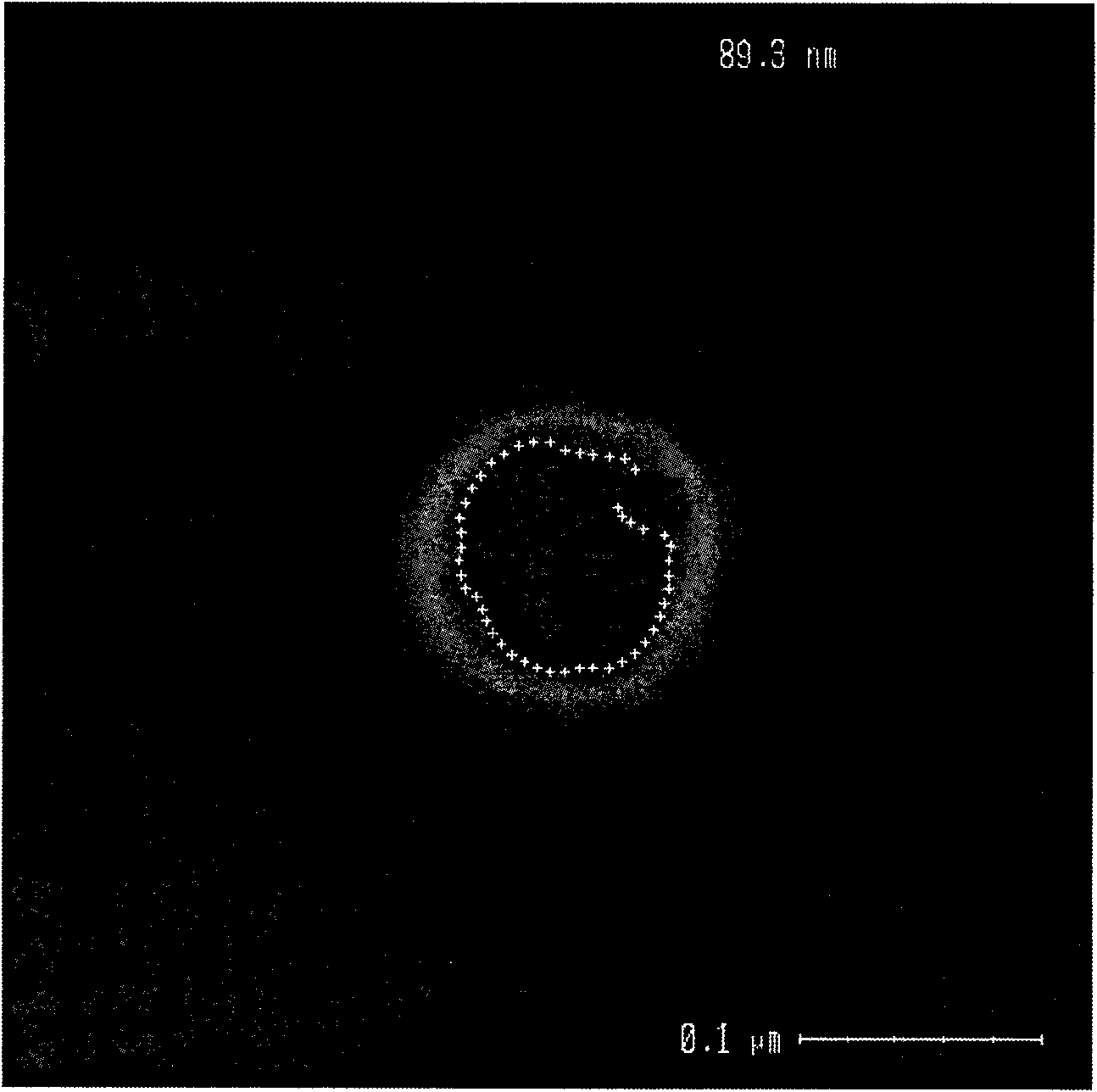
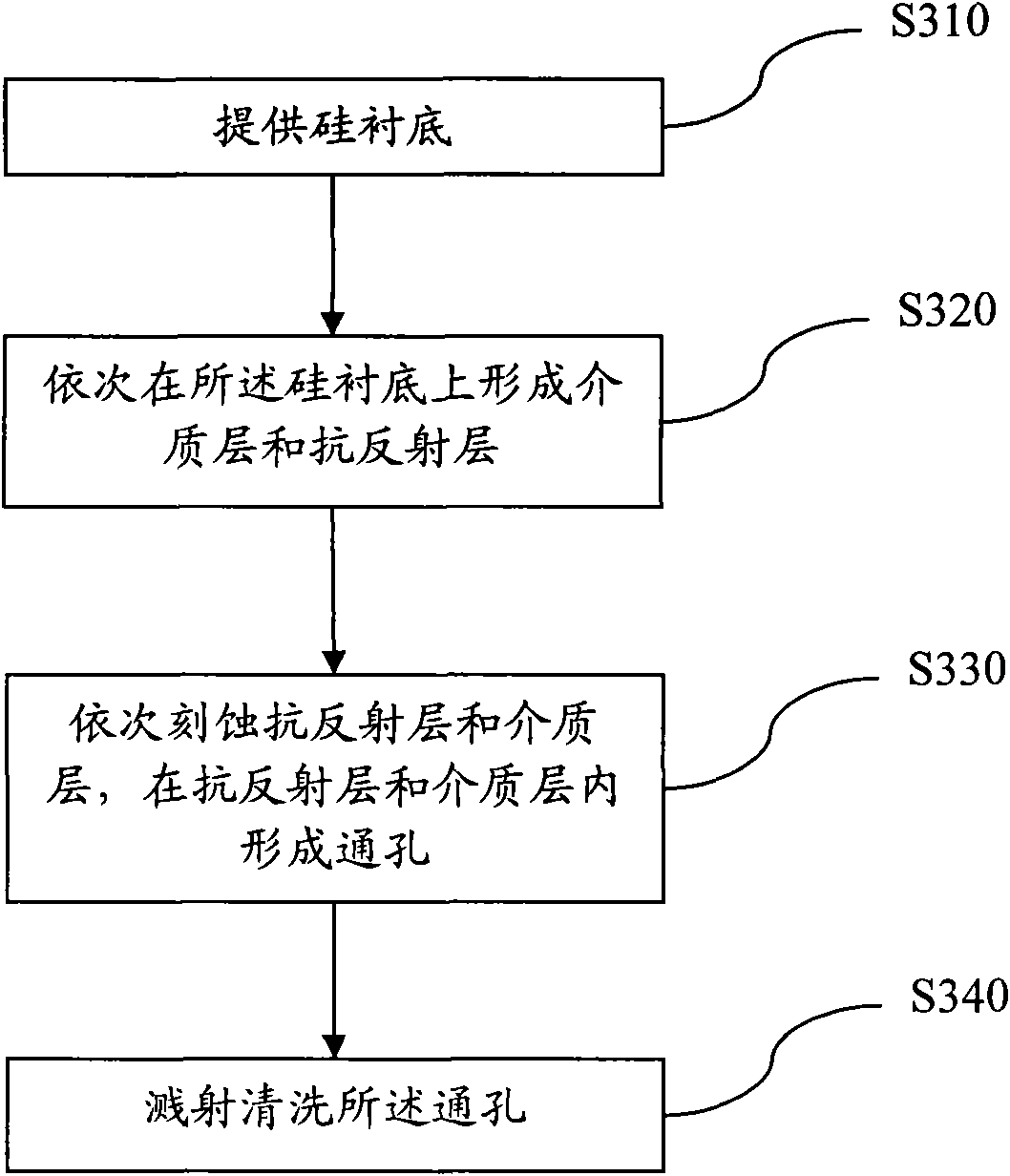
[0034] See image 3 , which shows a method for forming a through hole provided by an embodiment of the present invention. The method comprises the following steps:

[0035] S310: providing a silicon substrate;

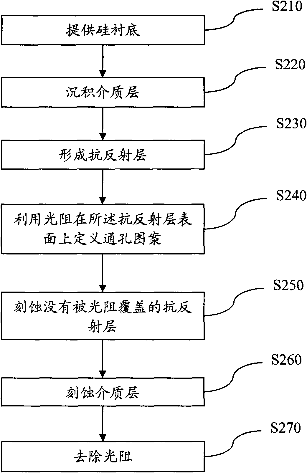
[0036] S320: sequentially forming a dielectric layer and an anti-reflection layer on the silicon substrate; forming a dielectric layer on the silicon substrate for forming a through hole, in this embodiment, the dielectric layer for forming a through hole is an oxide silicon layer, the thickness of which is to between, for example An anti-reflection layer is formed on the above-mentioned medium layer for forming a pattern thereon, and a through-hole pattern is defined on the surface of the anti-reflection layer by using a pho...


PUM

PropertyMeasurementUnit
poweraaaaaaaaaa

Abstract

The invention discloses a through hole forming method, which comprises the following steps: providing a silicon substrate; forming a medium layer and an anti-reflection layer on the silicon substrate in sequence; etching the anti-reflection layer and the medium layer in sequence, and forming through holes in the anti-reflection layer and the medium layer; and sputtering and cleaning the through holes. In the through hole forming method, a sputtering and cleaning step is added after a main through hole etching step so as to remove redundant polymers generated in the etching process and byproducts generated by etching light resistors to ensure that the side walls of the through holes are smooth and the edges thereof are clear, and thereby, the resistance distribution of the through holes is even.

Description

technical field [0001] The invention relates to the field of semiconductor manufacturing, in particular to a method for forming a through hole. Background technique [0002] With the development of semiconductor manufacturing process technology, the precision of semiconductor integrated circuits has reached the deep submicron size, which makes the integration degree of semiconductor devices and the complexity of manufacturing process continue to increase. Among them, the through hole is used as a channel for the interconnection of multi-layer metal layers and the connection between the active area of ​​the semiconductor device and the external circuit. Due to its important role in the structure of the semiconductor device, the precision requirements for the through hole etching process technology are also constantly increasing improve. [0003] In the prior art, in the process of forming through holes, especially when forming small-diameter through-holes, the polymer produc...

Claims


Application Information

Patent Timeline
Patent Type & Authority Applications(China)
IPC IPC(8): H01L21/768H01L21/311H01L21/3105
Inventor 赵林林沈满华
Owner SEMICON MFG INT (SHANGHAI) CORP
Why Eureka
Try Eureka