Patterned conducting element

A conductive element and patterning technology, which is applied in the field of preparing patterned conductive elements based on carbon nanotubes, can solve the problems of small resistance value range, poor durability, and increased resistance, achieve uniform resistance value distribution, and improve durability. Effect

Inactive Publication Date: 2012-12-12
TIANJIN FUNA YUANCHUANG TECH +1
View PDF6 Cites 4 Cited by
  • Summary
  • Abstract
  • Description
  • Claims
  • Application Information

AI Technical Summary

Problems solved by technology

However, after the ITO layer is continuously bent, the resistance at the bend increases. As a transparent conductive layer, it has the disadvantages of insufficient mechanical and chemical durability, and there is a phenomenon of uneven resistance and a small range of resistance values.
As a result, existing touch screens have disadvantages such as poor durability, low sensitivity, and poor accuracy.
Moreover, as a transparent conductive layer, the ITO layer is usually prepared by processes such as ion beam sputtering or evaporation, so the preparation cost of the ITO layer is relatively high.
The method of patterning the ITO layer is usually laser etching, which not only has high preparation cost, but also has low preparation efficiency.

Method used


Image

  • Patterned conducting element
  • Patterned conducting element
  • Patterned conducting element

Examples


Embodiment Construction

[0017] The patterned conductive element provided by the present invention and its preparation method will be further described in detail below with reference to the accompanying drawings and specific embodiments.

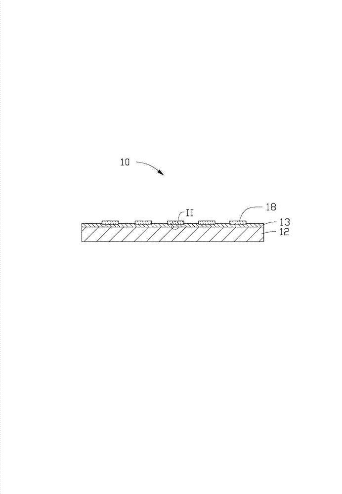
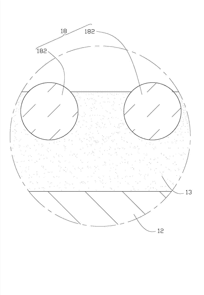
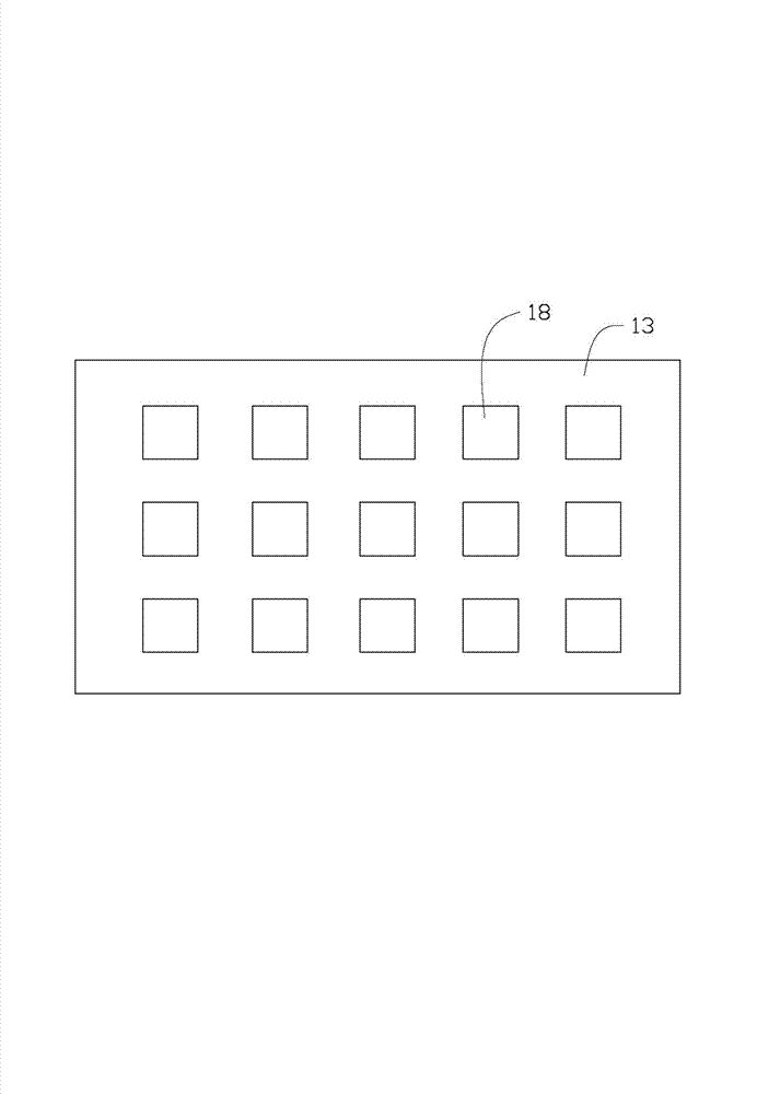
[0018] see figure 1 , the embodiment of the present invention provides a patterned conductive element 10 , which includes a substrate 12 , an adhesive layer 13 and a patterned carbon nanotube layer 18 . The adhesive layer 13 is disposed on a surface of the base 12 . The patterned carbon nanotube layer 18 is disposed on a surface of the adhesive layer 13 and fixed on the surface of the substrate 12 through the adhesive layer 13 .

[0019] The base 12 is mainly used as a support, and it can be a curved or flat structure. The base 12 has proper light transmittance. The base 12 may be formed from a rigid material or a flexible material. Specifically, the hard material may be selected from glass, quartz, diamond, or plastic. The flexible material can be selected fro...


PUM

PropertyMeasurementUnit
thicknessaaaaaaaaaa
thicknessaaaaaaaaaa
thicknessaaaaaaaaaa

Abstract

The invention relates to a patterned conducting element. The patterned conducting element specifically comprises a base, an adhesive layer and a patterned carbon nanotube layer, the adhesive layer is arranged on one surface of the base, and the surface of the patterned carbon nanotube layer is partly embedded in the adhesive layer and is partly exposed outside the adhesive layer.

Description

technical field [0001] The invention relates to a patterned conductive element, in particular to a method for preparing a patterned conductive element based on carbon nanotubes. Background technique [0002] Transparent conductive elements, especially patterned conductive elements, are important elements of various electronic devices, such as touch screens, liquid crystal displays, field emission display devices, and the like. [0003] A patterned conductive element in the prior art includes a substrate and a patterned indium tin oxide layer (ITO layer) formed on the surface of the substrate. However, after the ITO layer is continuously bent, the resistance at the bend increases. As a transparent conductive layer, it has the disadvantages of insufficient mechanical and chemical durability, and there is a phenomenon of uneven resistance and a small range of resistance values. . As a result, existing touch screens have disadvantages such as poor durability, low sensitivity, ...

Claims


Application Information

Patent Timeline
Patent Type & Authority Applications(China)
IPC IPC(8): H01B5/14H01B1/04
Inventor 郑嘉雄黄柏山施博盛胡君怡赵志涵吴志笙
Owner TIANJIN FUNA YUANCHUANG TECH
Why Eureka
Try Eureka