Method for selectively doping emitting stage on surface of crystalline silicon cell film

A technology on the surface of crystalline silicon cells and silicon wafers, applied to circuits, electrical components, semiconductor devices, etc., can solve problems such as difficulty in further improvement, limitation of cell conversion efficiency, lack of selective emission levels, etc., and achieve an increase in conversion efficiency , Improve the conversion efficiency, the effect of large profits

Active Publication Date: 2015-01-07
EGING PHOTOVOLTAIC TECHNOLOGY CO LTD
View PDF7 Cites 0 Cited by
  • Summary
  • Abstract
  • Description
  • Claims
  • Application Information

AI Technical Summary

Problems solved by technology

Although this doping junction method enables solar cells to adopt mature screen printing technology to meet the requirements of industrial mass production, however, the gate surface of the cell does not have a selective emission level due to the surface doping junction. , so the conversion efficiency of the cell is limited and it is difficult to further improve

Method used


Image

  • Method for selectively doping emitting stage on surface of crystalline silicon cell film
  • Method for selectively doping emitting stage on surface of crystalline silicon cell film
  • Method for selectively doping emitting stage on surface of crystalline silicon cell film

Examples


Embodiment Construction

[0033] A specific embodiment of the present invention will be described below by taking a monocrystalline silicon solar cell as an example.

[0034] attached figure 1 ~ attached Figure 11 as the main production process.

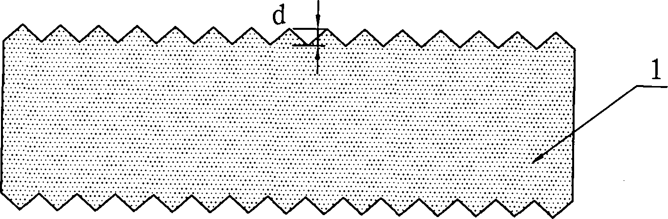
[0035] figure 1 is a schematic diagram of the structure of p-type monocrystalline silicon wafer 1 after texturing treatment, in figure 1 Among them, the thickness of the p-type single crystal silicon wafer 1 is 180-200 microns, and its resistivity is between 1-5 ohm·cm. After texturing, the depth d formed on the upper and lower surfaces of the p-type single crystal silicon wafer 1 is 3-5 micron suede;

[0036] The present invention starts from the p-type monocrystalline silicon chip 1 after the texturing treatment, and its specific steps are as follows:

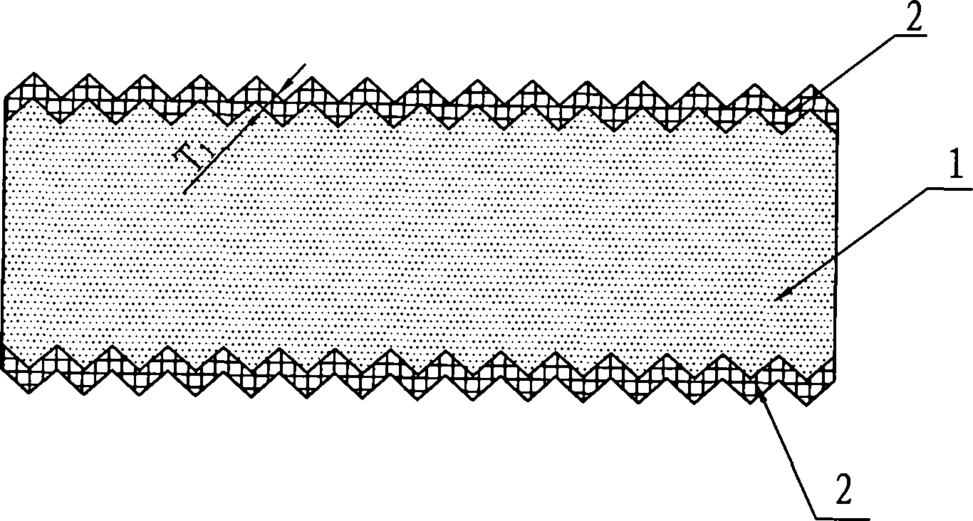
[0037] The first step, dry masking: put the textured silicon wafer 1 into an oxidation furnace at 1000°C-1100°C, pass in oxygen for dry oxidation, the oxidation time is 10 minutes, and epitaxy on the u...


PUM


Abstract

The invention relates to a method for selectively doping an emitting stage on the surface of a crystalline silicon cell film, comprising the steps of dry-method masking, wet-method masking, laser etching on a shallow slot, grid shallow slot scouring, heavy doping of the grid shallow slot, clearing phosphor and removing film, surface light doping and scouring. As the traditional one-step masking is changed into masking by using a dry method and a wet method, two basic requirements of subsequent heavy doping and light doping are satisfied; an interface between a mask and a silicon slice is tightly combined, which can effectively resist diffusion for selective doping; the mask has enough thickness which can bear the reduction effect of scouring; in a same oxidation furnace, the method for combining dry-method oxidation with wet-method oxidation is adopted, thereby ensuring the favorable quality of the contact surface of a dry-method oxidization mask and the silicon slice; the wet-method oxidization ensures that the growing speed of the mask is improved by 10 times, which enables the mask to grow to the thickness of about 1 mu m in short time, thereby overcoming the defect of slow epitaxial growth of dry-method oxidization, remarkably shortening the time of the production process, and improving the yield.

Description

【Technical field】 [0001] The invention relates to a manufacturing process of a crystalline silicon solar cell, in particular to a method for manufacturing a selective emission level by doping the surface of a crystalline silicon solar cell. 【Background technique】 [0002] With the growing demand for renewable green energy, crystalline silicon solar cell technology has been greatly promoted and developed. The manufacturing process of crystalline silicon solar cells includes surface texturing, surface doping junction, antireflection film deposition, positive and negative electrode formation and other processes. In the industrialized manufacturing method, the silicon chip surface doping junction scheme is the main step that limits the improvement of the cell conversion efficiency. At present, the current surface doping and junction making process of solar cells using the screen printing process is as follows: [0003] The surface of the electrode is directly doped on the sili...

Claims


Application Information

Patent Timeline
Patent Type & Authority Patents(China)
IPC IPC(8): H01L31/18
CPCY02P70/50
Inventor 孙剑波孙铁囤叶庆好
Owner EGING PHOTOVOLTAIC TECHNOLOGY CO LTD
Why Eureka
Try Eureka