Method for improving breakdown voltage of LDMOS devices

A technology of breakdown voltage and devices, which is applied in semiconductor devices, semiconductor/solid-state device manufacturing, circuits, etc., can solve problems such as increased breakdown voltage of devices, achieve the effects of increasing breakdown voltage, increasing process complexity, and saving production costs

Active Publication Date: 2010-11-03
SHANGHAI HUAHONG GRACE SEMICON MFG CORP
View PDF0 Cites 15 Cited by
  • Summary
  • Abstract
  • Description
  • Claims
  • Application Information

AI Technical Summary

Problems solved by technology

However, in this structure, there are also unavoidable problems, that is, because the gate is an equipotential body, the electric force line will be nearly perpendicular to its surface, and the equipotential line will be nearly parallel to its surface, so that from the junction of PF and PA The potent...

Method used


Image

  • Method for improving breakdown voltage of LDMOS devices
  • Method for improving breakdown voltage of LDMOS devices
  • Method for improving breakdown voltage of LDMOS devices

Examples


Embodiment Construction

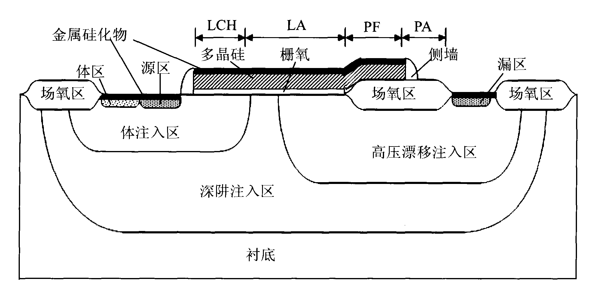
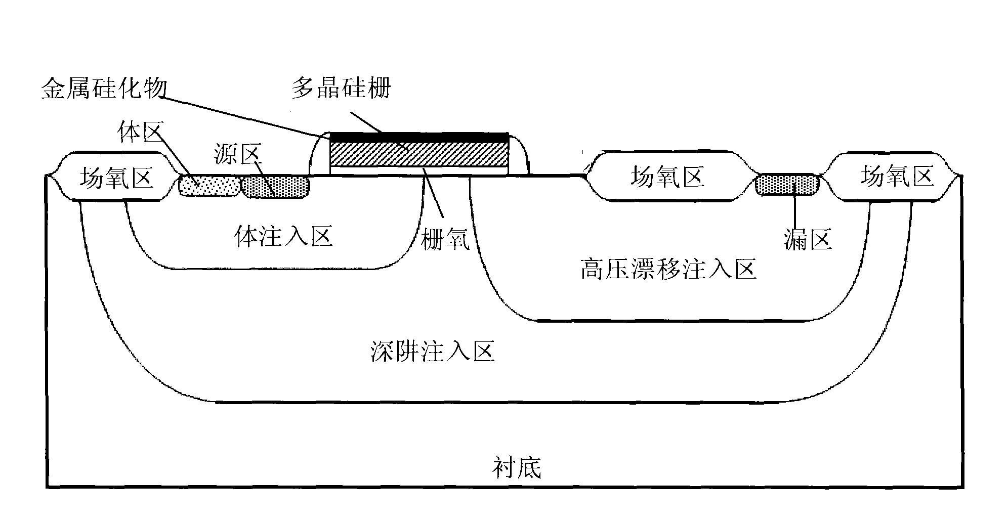
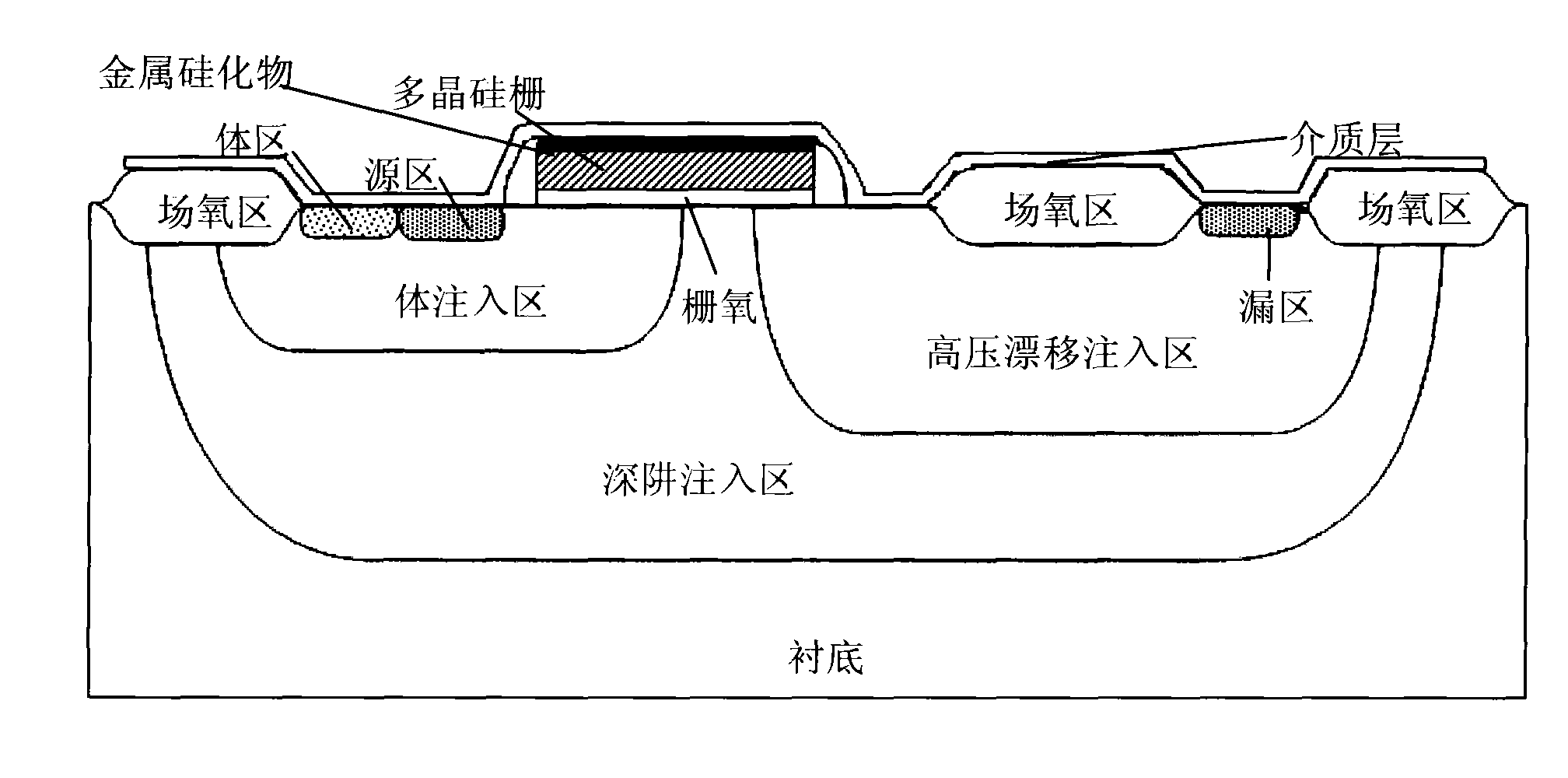
[0016] In the manufacture of semiconductor devices, the preparation process of the main structure of the device is usually called the front-end process, while the metal interconnection between multiple devices in the chip is called the back-end process. The method for improving the breakdown voltage of the LDMOS device of the present invention is mainly divided into two parts:

[0017] One is to prepare the gate structure of the LDMOS device in the previous stage according to the conventional method (the gate structure generally includes the underlying gate oxide, the polysilicon gate on the gate oxide, and the sidewalls on both sides of the above two layers of materials), the formed gate The structure is located above the area where the channel is expected to be formed in the LDMOS device and extends above the high-voltage drift injection region, and the gate structure is physically isolated from the field oxygen region located in the high-voltage drift injection region (see ...


PUM


Abstract

The invention discloses a method for improving breakdown voltage of LDMOS devices, in the process of a front-segment preparation grid structure by adopting a conventional method, a grid structure is arranged above the area of an LDMOS device channel, is extended above a high-voltage drifting injection area and is separated from a field oxide area of the high-voltage drifting injection area; in the rear-segment process, a dielectric layer is sedimentated firstly, and then a conductor layer is sedimentated, and then the dielectric layer and the conductor layer are etched, the dielectric layer and the conductor layer above the high-voltage drifting injection area are kept to form a suspending grid electrode electric-conduction equipotential body, one end of the equipotential body is arranged on the field oxide area in the high-voltage drifting injection area, and the other end is arranged above the grid structure and between one side of a channel area and one side of a beak part of the field oxide area in the high-voltage drifting injection area. The method can be integrated in the PIP, MIP or RPOLY process and can be integrated in a metal connecting line process. The method in the invention can obviously improve the breakdown voltage of the LDMOS devices.

Description

technical field [0001] The invention relates to a preparation method of an LDMOS device, in particular to a method for increasing the breakdown voltage of the LDMOS device. Background technique [0002] In the current LDMOS (Laterally Diffused Metal Oxide Field Effect Transistor) device structure, the polysilicon gate is generally extended to the upper end of the field oxygen region, which can prevent the polysilicon from extending only to the LA region, because the thin gate oxide in the LA region is prone to leaks. The voltage difference between the region and the gate is easier to break down, resulting in a problem with a smaller breakdown voltage of the device. figure 1 Shown is a common LDMOS device structure, in which the width LCH of the channel region is formed by the overlapping region of polysilicon and the low-voltage P well; the LA segment is the region on the drain region from the channel region to the field oxide region , including the beak part of the field o...

Claims


Application Information

Patent Timeline
IPC IPC(8): H01L21/336H01L21/822H01L29/92H01L21/768H01L29/49H01L21/027
Inventor 陈华伦罗啸韩峰陈瑜熊涛陈雄斌
Owner SHANGHAI HUAHONG GRACE SEMICON MFG CORP
Why Eureka
Try Eureka