Method for manufacturing solder lug

A fabrication method and technology for solder bumps, which are used in the manufacture of semiconductor/solid-state devices, electrical components, and electrical solid-state devices, etc., can solve the problems of abnormal bump shape, poor consistency of height and volume of solder bumps, etc. Consistency of rate, height and volume for easy-to-control effects

Active Publication Date: 2010-11-24
SEMICON MFG INT (SHANGHAI) CORP
View PDF0 Cites 6 Cited by
  • Summary
  • Abstract
  • Description
  • Claims
  • Application Information

AI Technical Summary

Problems solved by technology

[0015] The invention provides a method for manufacturing solder bumps to solve the problem of abnormal shape of bumps formed in the prior art and poor consistency of height and volume of solder bumps

Method used


Image

  • Method for manufacturing solder lug
  • Method for manufacturing solder lug
  • Method for manufacturing solder lug

Examples


Embodiment Construction

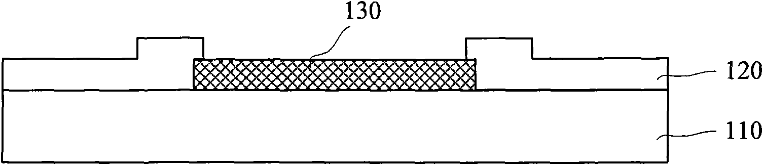
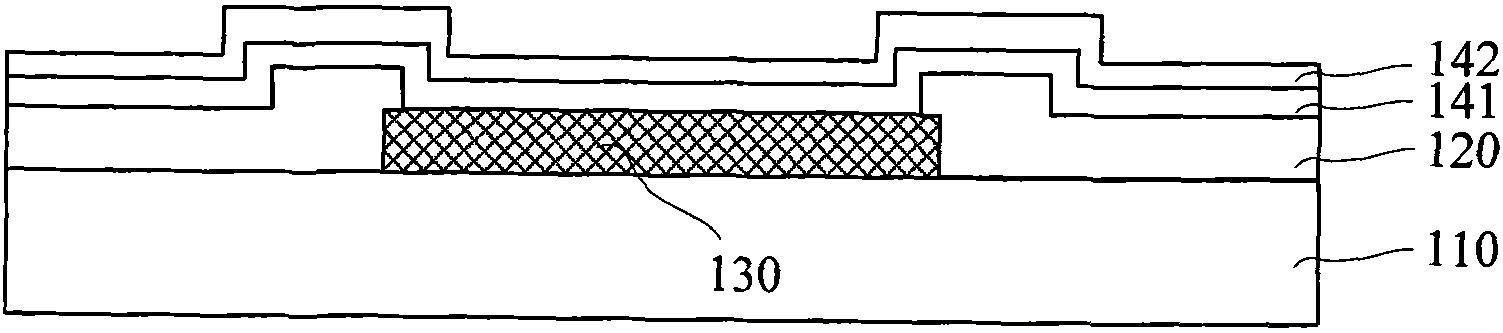
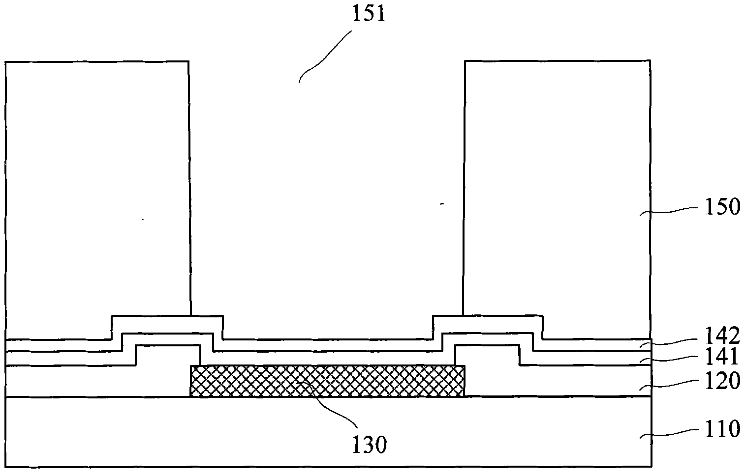
[0030] In order to make the purpose and features of the present invention more comprehensible, the specific implementation manners of the present invention will be further described below in conjunction with the accompanying drawings. It should be noted that the drawings are all in a very simplified form and use imprecise ratios, which are only used to facilitate and clearly assist the purpose of illustrating the embodiments of the present invention.

[0031] It will also be understood that when a layer is referred to as being "on" another layer or substrate, it can be directly on the other layer or substrate, or intervening layers may also be present. It will also be understood that when a layer is referred to as being "under" another layer, it can be directly under, and there may be one or more intervening layers. In addition, it will also be understood that when a layer is referred to as being "between" two layers, it can be the only layer between the two layers, or one or ...


PUM


Abstract

The invention discloses a method for manufacturing a solder lug. The method comprises the following steps: providing a semiconductor substrate with a pad; forming a metal laminate on the semiconductor substrate; forming a first photoresist layer on the metal laminate, and patterning the first photoresist layer to form a first opening which is positioned above the pad and exposed from the metal laminate; forming a metal electrode in the first opening; flattening the first photoresist layer and the surface of the metal electrode; forming a second photoresist layer on the first photoresist layer and the surface of the metal electrode, and patterning the second photoresist layer to form a second opening which is exposed from the metal electrode; forming a solder layer in the second opening; removing the first photoresist layer, the second photoresist layer and the metal laminate which is not covered by the metal electrode; and refluxing the solder layer to form bumps. In the method, high quality solder lug with accordant height and volume can be formed, and the yield of semiconductor devices can be improved.

Description

technical field [0001] The invention relates to the field of integrated circuit manufacturing, in particular to a method for manufacturing solder bumps. Background technique [0002] With the continuous development of integrated circuit technology, semiconductor devices are increasingly developing in the direction of miniaturization, intelligence, high performance, and high reliability. With the gradual reduction of the size of integrated circuit chips and the continuous improvement of integration, the electronics industry has put forward higher and higher requirements for integrated circuit packaging technology. Traditional packaging technology has become a bottleneck restricting the improvement of circuit performance, prompting the development of chip packaging technology from the original cutting and crimping technology to the current flip chip (Flip Chip) technology. [0003] Flip-chip technology is to form solder bumps on the chip's bonding pad (Bond Pad) after the chi...

Claims


Application Information

Patent Timeline
Patent Type & Authority Applications(China)
IPC IPC(8): H01L21/60H01L23/482
CPCH01L24/11H01L2224/11H01L2924/01322H01L2924/14H01L2924/00H01L2924/00012
Inventor 李润领童沙丹司伟吴俊徐王津洲
Owner SEMICON MFG INT (SHANGHAI) CORP
Why Eureka
Try Eureka