Method for enhancing reliability of chip welding spot, printed circuit board and electronic device

A printed circuit board and enhanced chip technology, which is applied to printed circuits, printed circuits connected with non-printed electrical components, printed circuits assembled with electrical components, etc., can solve the problem of reducing manufacturing efficiency, increasing equipment cost investment, and increasing process flow and other issues, to achieve the effect of improving manufacturing efficiency, reducing equipment cost investment, and reducing process flow

Active Publication Date: 2010-11-24
HUAWEI DEVICE CO LTD
View PDF3 Cites 28 Cited by
  • Summary
  • Abstract
  • Description
  • Claims
  • Application Information

AI Technical Summary

Problems solved by technology

[0004] At the same time, because the existing solder paste printing method cannot meet the high-density printing requirements of 0.30mm pitch CSP chips, the Dipping Flux process solution is adopted, but due to reliability requirements, Underfill protection is still required after Dipping Flux Program
[0005] In the research on the prior art, the inventor found that: since the existing methods for enhancing the reliability of chip solder joints all require the Underfill process, and the Underfill process is not compatible with the SMT process, so in order to complete the Underfill, it is necessary to add after PCBA processing Underfill related equipment not only increases equipment cost investment, but also increases process flow and reduces manufacturing efficiency

Method used


Image

  • Method for enhancing reliability of chip welding spot, printed circuit board and electronic device
  • Method for enhancing reliability of chip welding spot, printed circuit board and electronic device
  • Method for enhancing reliability of chip welding spot, printed circuit board and electronic device

Examples


Embodiment Construction

[0028] The following will clearly and completely describe the technical solutions in the embodiments of the present invention with reference to the accompanying drawings in the embodiments of the present invention. Obviously, the described embodiments are only some, not all, embodiments of the present invention. Based on the embodiments of the present invention, all other embodiments obtained by persons of ordinary skill in the art without creative efforts fall within the protection scope of the present invention.

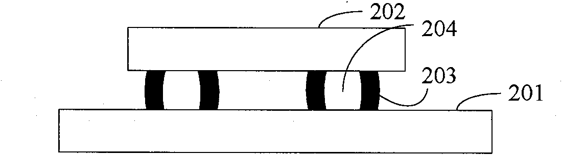
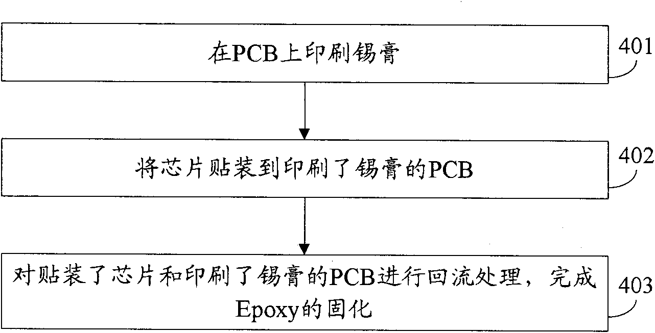
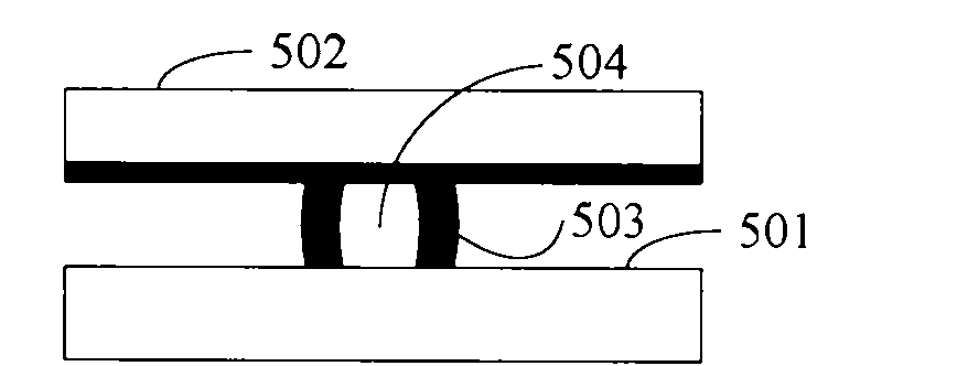
[0029] First introduce the method for enhancing the reliability of chip solder joints provided by the embodiment of the present invention, figure 1 The process flow of the method for enhancing the reliability of chip solder joints provided by an embodiment of the present invention is described. This embodiment describes the process of enhancing the reliability of top-layer chip solder joints in the process flow of POP, including:

[0030] 101. Dip Epoxy Flux onto t...


PUM


Abstract

The invention relates to PCBA processing and discloses a method for enhancing the reliability of a chip welding spot, a printed circuit board and an electronic device. The method for enhancing the reliability of the chip welding spot comprises the following steps of: dipping an epoxy resin soldering flux on a welding foot of the chip or coating the epoxy resin soldering flux on a bonding pad corresponding to the welding foot of the chip, and attaching the chip to the bonding pad; and performing reflux treatment on the bonding pad to which the chip is attached and finishing curing the epoxy resin soldering flux. The method reduces the investment of the device and improves the manufacturing efficiency because an Underfill process is unnecessary.

Description

technical field [0001] The invention relates to the processing of assembled printed circuit board (PCBA: Printed Circuit Board Assembly), in particular to a method for enhancing the reliability of chip solder joints, a printed circuit board and electronic equipment. Background technique [0002] Multi-functionalization and miniaturization have become the main development trend and technical requirements of personal consumer electronics products such as mobile phones and wireless network cards; therefore, in order to enhance product functions and reduce product volume, consumer electronics chip manufacturers start from Pitch chip size packaging (CSP: Chip Scale Packaging) is gradually developing to 0.40mm pitch or even 0.30mm pitch CSP, and three-dimensional assembly technology such as stacked packaging (POP: Package On Package) chip stacking technology is introduced at the same time. To improve the layout density of PCBA, the thickness of printed circuit board (PCB: Printed ...

Claims


Application Information

Patent Timeline
Patent Type & Authority Applications(China)
IPC IPC(8): H01L21/60H01L23/498H05K1/18H05K3/34
CPCH01L23/293H01L2224/16227H01L2224/03828H01L24/13H01L2924/01057H01L21/563H01L2224/131H01L2924/0105H01L2924/014H01L2224/81862H01L2224/81905H05K13/04H01L2224/1369H01L2224/16225H01L2924/01006H01L2224/11822H01L2224/81815H01L2224/81355H01L24/16H01L2224/81011H05K1/181H01L24/81H01L24/11H01L2224/0401
Inventor 罗德威
Owner HUAWEI DEVICE CO LTD
Why Eureka
Try Eureka