TFT (Thin Film Transistor) array structure and manufacturing method thereof

A technology of array structure and manufacturing method, applied in semiconductor/solid-state device manufacturing, semiconductor/solid-state device components, semiconductor devices, etc., to reduce difficulty and cost, solve crosstalk and distortion, and improve yield

Inactive Publication Date: 2010-11-24
SHANGHAI TIANMA MICRO ELECTRONICS CO LTD
View PDF1 Cites 5 Cited by
  • Summary
  • Abstract
  • Description
  • Claims
  • Application Information

AI Technical Summary

Problems solved by technology

[0005] In order to solve the above problems, the present invention provides a TFT array structure and a manufacturing method thereof, which can simplify the production process of the TFT array, reduce production costs, and solve the problems of crosstalk and distortion between data lines, and improve the yield of the TFT array structure

Method used


Image

  • TFT (Thin Film Transistor) array structure and manufacturing method thereof
  • TFT (Thin Film Transistor) array structure and manufacturing method thereof
  • TFT (Thin Film Transistor) array structure and manufacturing method thereof

Examples


no. 1 example

[0048] In-plane switching liquid crystal display (IPS-LCD) is one of the mainstream wide viewing angle LCD technologies. The difference from twisted array liquid crystal display (TN-LCD) is that the common electrode and pixel electrode of IPS-LCD are fabricated on the substrate. On the same side, the common electrode and the pixel electrode are driven by the horizontal driving electric field, which can make the liquid crystal molecules rotate on the plane and greatly increase the viewing angle.

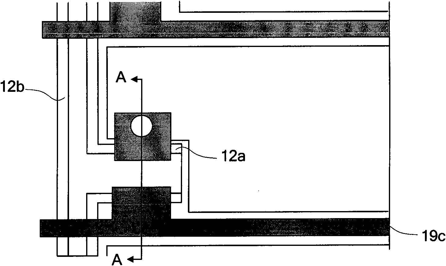
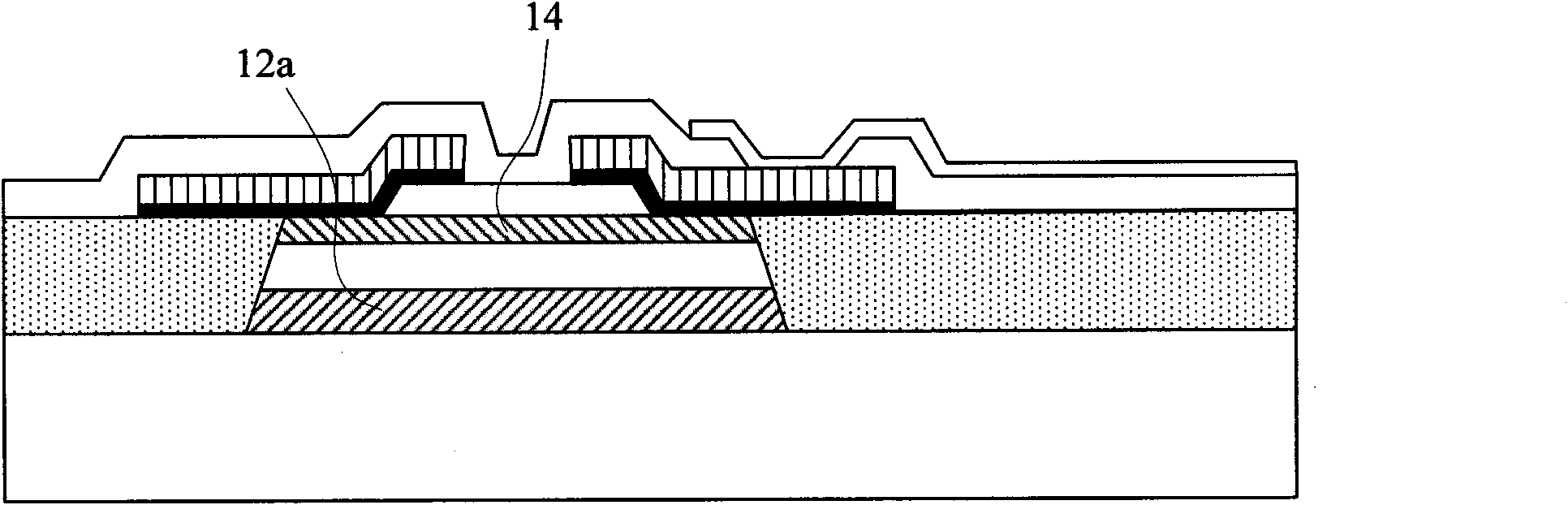
[0049] Please refer to Figure 4 to Figure 5 ,in, Figure 4 It is a top view of the TFT array structure proposed in the first embodiment of the present invention, Figure 5 for Figure 4 Sectional view of part A-A in middle, Figure 6 for Figure 4 Sectional view of part B-B in middle.

[0050] As shown in the figure, the TFT array structure 200 that can be used for IPS-LCD includes: a substrate 210, a gate line 224 and a common electrode 222 formed on the substrate 210, a data l...

no. 2 example

[0073] Please refer to Figure 8 to Figure 10 ,in, Figure 8 It is a top view of the TFT array structure proposed in the second embodiment of the present invention, Figure 9 for Figure 8 Sectional view of part A-A in middle, Figure 10 for Figure 8 Sectional view of part B-B in middle.

[0074]As shown in the figure, the TFT array structure 300 that can be used for TN-LCD includes: a substrate 310, a gate line 324 and a common electrode 322 formed on the substrate 310, a data line 383 intersecting with the gate line 324; The common electrode 322 and the insulating layer 361 on the substrate 310; the TFT formed at the intersection of the gate line 324 and the data line 383, wherein the TFT includes a gate 323 integrated with the gate line 324, which is sequentially formed on the The gate insulating layer 331 and the semiconductor layer 341 on the gate 323, the drain 381 and the source 382 integrated with the data line 383; wherein, the gate between two data lines 383 an...


PUM


Abstract

The invention provides a TFT array structure and a manufacturing method thereof. The TFT array structure comprises a base plate, a grid line and a common electrode which are formed on the base plate, data lines crossed with the grid line, insulating layers formed on the common electrode and the base plate, and TFTs formed on the intersections of the grid line and the data lines, wherein each TFT comprises a grid forming into a whole with the grid line, a grid insulating layer and a semiconductor layer which are sequentially formed on the grid, a drain electrode and a source electrode forming into a whole with the data lines; the semiconductor layer on the grid line between the intersections of two data lines and the grid line is at least partially etched. Therefore, when voltage signals of the two data lines are different, current does not flow between the two data lines. By the invention, the manufacturing cost of the TFT array structure can be reduced; the problems of crosstalk and distortion between the data lines are solved; and the yield is enhanced advantageously.

Description

technical field [0001] The invention relates to flat panel display technology, in particular to a thin film transistor (TFT) array structure and a manufacturing method thereof. Background technique [0002] At present, the application of flat-panel display technology in daily life is becoming more and more common. For example, mobile terminals such as notebook computers and mobile phones, digital photo frames, and GPS navigators all need to be applied to flat-panel display technology. Although liquid crystal display technology (LCD) occupies a dominant position in the field of flat panel display technology, technologies such as organic light-emitting diodes (OLED) and electronic ink (E-INK) are also developing rapidly. [0003] Flat panel display devices are classified into passive matrix (PM) flat panel display devices using a passive driving method and active matrix (AM) flat panel display devices using active driving according to driving methods. Among them, an active ma...

Claims


Application Information

Patent Timeline
Patent Type & Authority Applications(China)
IPC IPC(8): H01L27/12H01L23/528H01L21/84H01L21/768
Inventor 袁剑峰赵本刚
Owner SHANGHAI TIANMA MICRO ELECTRONICS CO LTD
Why Eureka
Try Eureka