Charge pump capable of solving problems of charge distribution and current mismatching

A technology of charge distribution and charge pump, which is applied in the field of charge pump, can solve problems such as damage to output clock noise performance, charge pump charge distribution, current mismatch, etc., and achieve perfect charge and discharge current matching, convenient operation, and simple structure.

Inactive Publication Date: 2010-11-24
苏州科山微电子科技有限公司
View PDF5 Cites 21 Cited by
  • Summary
  • Abstract
  • Description
  • Claims
  • Application Information

AI Technical Summary

Problems solved by technology

When M1 is in the cut-off state, the voltage of VCTRL will be changed by the control of the phase-locked loop. When the UP signal changes from high to low, M1 will be turned on. At the moment of conduction, if the voltage of VCTRL is not equal to the voltage of point N1, It will inevitably lead to the redistribution of charge between VCTRL and N1. The result of this charge redistribution is to generate ripples in the VCTRL voltage. This ripple will cause irregular jitter in the VCO signal, thereby seriously damaging the noise of the output clock. performance
The same problem exists at the M2 and N2 side, which is the charge distribution problem o

Method used


Image

  • Charge pump capable of solving problems of charge distribution and current mismatching
  • Charge pump capable of solving problems of charge distribution and current mismatching
  • Charge pump capable of solving problems of charge distribution and current mismatching

Examples


Embodiment Construction

[0017] The present invention will be further described below in conjunction with the accompanying drawings and embodiments.

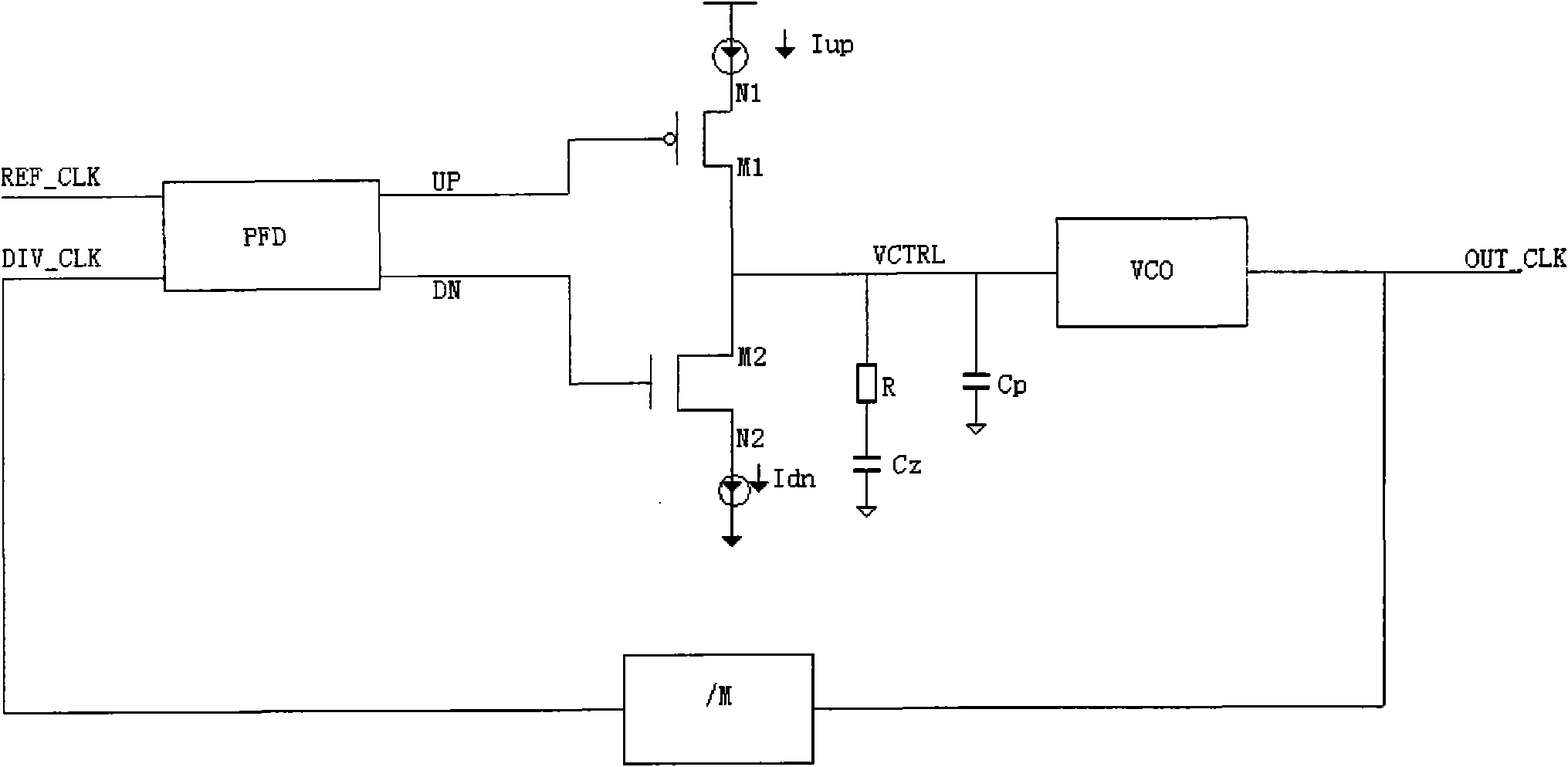
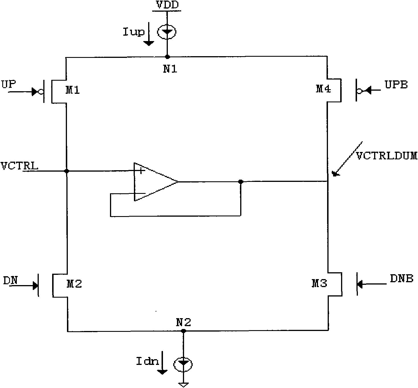
[0018] figure 2 The circuit structure can be used to solve the problem of charge distribution, such as figure 2 As shown, there is an operational amplifier inside, the positive input and output of the operational amplifier are respectively connected to the two branches of the differential charge pump input structure, and its negative input and output are shorted to form a unity gain buffer device. The PFD output signal adopts a differential form. When UP=high, M1 is in the off state, but when UPB=low, M4 is in the on state, so the voltage of N1 and the voltage of VCTRLDUM are always equal, because figure 2 The operational amplifier in the circuit adopts the connection mode of unity gain buffer, so that no matter how VCTRL changes, the voltage of VCTRLDUM follows the change of VCTRL, that is, in any state, the voltages of N1, VCTRLDUM and VCTRL are ...


PUM


Abstract

The invention relates to a charge pump capable of solving problems of charge distribution and current mismatching. The charge pump is provided with a charge pump core circuit, a current copy feedback circuit, and a seventh NMOS transistor. The charge pump core circuit comprises a differential charge pump input structure, a first PMOS transistor, a first NMOS transistor and an operational amplifier, wherein the differential charge pump input structure consists of a sixth PMOS transistor, a seventh PMOS transistor, an eighth PMOS transistor and a ninth PMOS transistor. A grid of a third NMOS transistor is connected with a positive input end of the operational amplifier; the source and grid of a third PMOS transistor are connected with the sources and grids of the first PMOS transistor and a second PMOS transistor respectively; the source and grid of a fifth NMOS transistor are connected with the sources and grids of the first NMOS transistor and a second NMOS transistor respectively; the grid of a fourth NMOS transistor is connected with the drain of a fifth PMOS transistor; and the drains and sources of the third PMOS transistor and the fourth PMOS transistor are in short circuit. The grid and source of the seventh NMOS transistor are connected with the grid and source of the first NMOS transistor. The charge pump cannot generate ripple vibration, can realize perfect charging and discharging current matching, and has the advantages of simple structure and convenient operation.

Description

Technical field: [0001] The invention relates to a charge pump which can solve the problems of charge distribution and current mismatch, and is used in a phase-locked loop (PLL). Background technique: [0002] exist figure 1 In the phase-locked loop (PLL), the signals input by the phase / frequency discriminator (PFD) are the reference clock and the clock output by the divider respectively. The PFD generates error signals UP and DN by comparing the frequency and phase of the two signals. The error signal can generate the DC control voltage VCTRL used to control the output frequency of the voltage-controlled oscillator (VCO) through the charge pump and the loop filter. This is an automatic feedback system. When the feedback system is locked, REF_CLK=DIV_CLK=OUT_CLK / M, and the purpose of generating a high frequency signal through a low frequency signal is realized. As a very critical component in the PLL system, the design of the charge pump usually encounters two important pr...

Claims


Application Information

Patent Timeline
IPC IPC(8): H02M3/07
Inventor 梅海涛孙礼中
Owner 苏州科山微电子科技有限公司
Why Eureka
Try Eureka