Solar panel and encapsulation process

A technology for solar panels and packaging technology, applied in circuits, photovoltaic power generation, electrical components, etc., can solve the problems of uneven packaging, high rejection rate, air bubbles, etc., and achieve the effect of closed flat, low rejection rate, and low hardness

Active Publication Date: 2010-12-15
HANGZHOU SOLAR PHOTOELECTRICITY
View PDF7 Cites 18 Cited by
  • Summary
  • Abstract
  • Description
  • Claims
  • Application Information

AI Technical Summary

Problems solved by technology

[0008] Another problem to be solved by the present invention is that the existing solar cell panels packaged with PET materials in the prior art have the problems of uneven packaging, bubbles, and high rejection rate. Packaging process for solar panels with low scrap rate

Method used


Image

  • Solar panel and encapsulation process
  • Solar panel and encapsulation process
  • Solar panel and encapsulation process

Examples


Embodiment 1

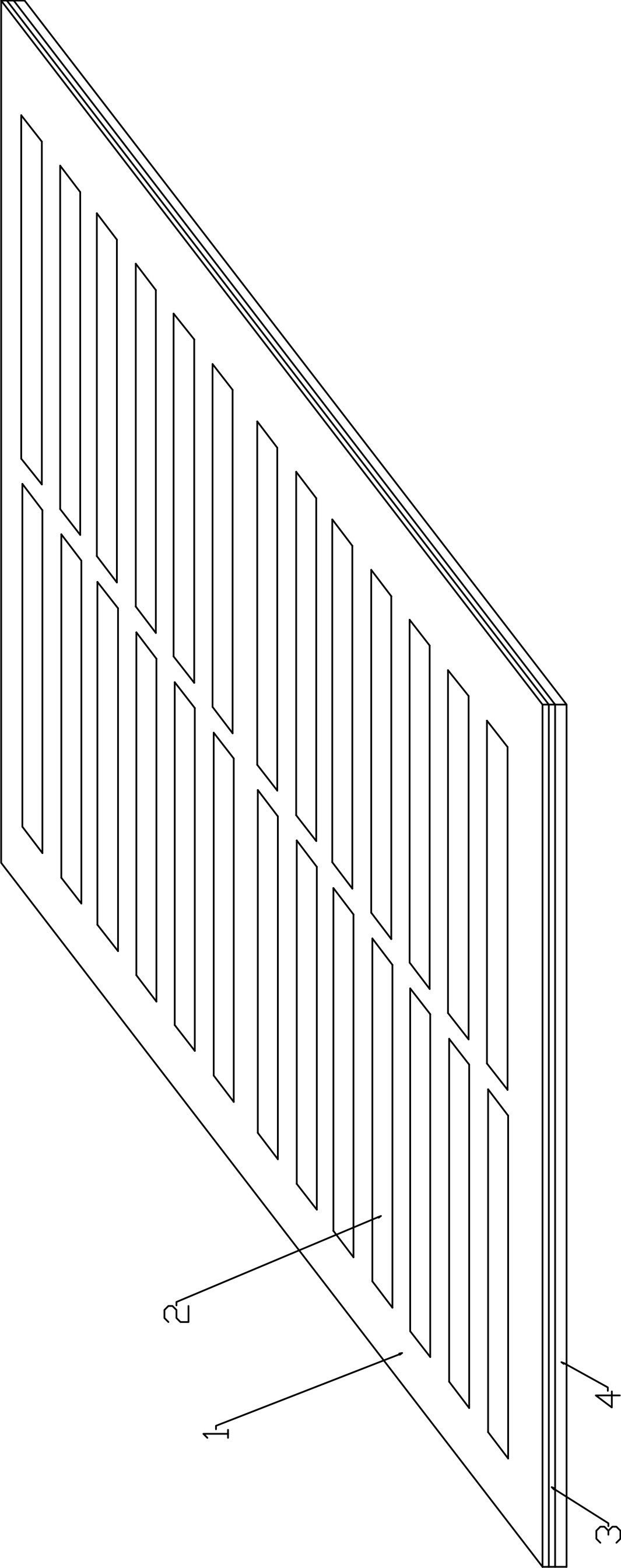
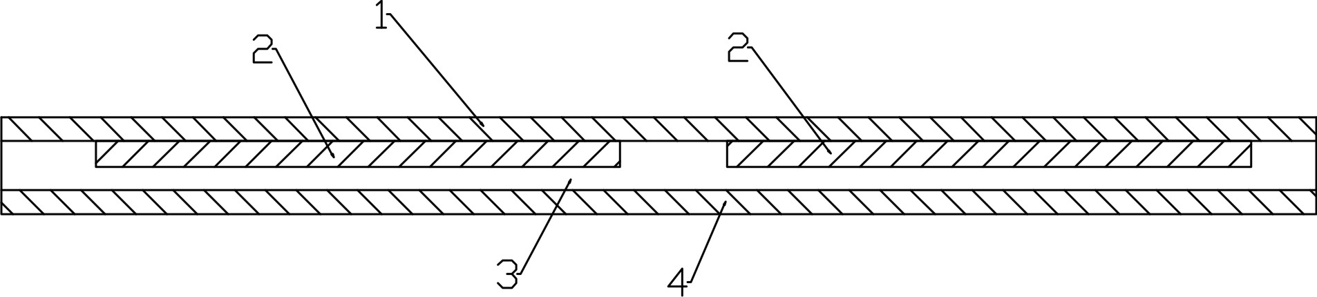
[0032] Such as figure 1 , figure 2 As shown, the present invention is a solar cell panel, including a silicon wafer 2, the silicon wafer is embedded in a layer of EVA glue layer 3, and the EVA glue layer is respectively connected with the PCB board 4 and the transparent layer of PET material 1 phase bonding. The front, rear, left, and lower sides of the silicon wafer are arranged in the EVA glue layer, the thickness of the EVA glue layer is 0.3-0.5mm, and the upper side of the silicon wafer is attached to the lower side of the light-transmitting layer of PET material. The PCB board is provided with positive and negative electrode printed lines connected with the positive and negative electrodes of the silicon chip.

[0033] The solar panel is manufactured through the following process, including the following steps:

[0034] The first step is to arrange the light-transmitting layers of PCB board, sheet EVA hot melt adhesive, silicon wafer, sheet EVA hot melt adhesive, and PET mat...

Embodiment 2

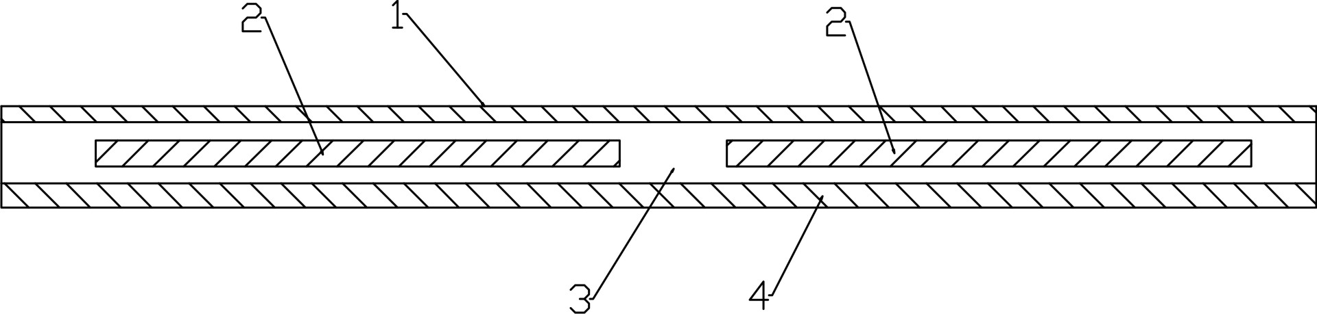
[0042] Such as image 3 As shown, the present invention is a solar cell panel, including a silicon wafer 2, the silicon wafer is embedded in a layer of EVA glue layer 3, and the EVA glue layer is respectively connected with the PCB board 4 and the transparent layer of PET material 1 phase bonding. The front, rear, left, and lower sides of the silicon wafer are arranged in the EVA glue layer, the thickness of the EVA glue layer is 0.3-0.5mm, and the upper side of the silicon wafer is attached to the lower side of the light-transmitting layer of PET material. The PCB board is provided with positive and negative electrode printed lines connected with the positive and negative electrodes of the silicon chip.

[0043] The solar panel is manufactured through the following process, including the following steps:

[0044] The first step is to arrange the light-transmitting layers of PCB board, sheet EVA hot melt adhesive, silicon wafer, sheet EVA hot melt adhesive, and PET material from ...


PUM


Abstract

The invention relates to a solar panel and an encapsulation process. The solar panel comprises a silicon wafer, wherein the back of the silicon wafer is adhered to a printed circuit board (PCB) board; a polythylene terephthalate (PET) material light-transmitting layer is arranged on the upside of the silicon wafer; and the PCB board is provided with anode and cathode printed coils which are connected with the anode and cathode of the silicon wafer. The encapsulation process of the solar panel comprises the following steps of: firstly, clamping the silicon wafer and flake-like ethylene vinyl acetate (EVA) hot melt glue between the PCB board and the PET material light-transmitting layer and placing the whole body in a vacuum laminating machine; secondly, vacuumizing the vacuum laminating machine and then heating materials to be processed in the vacuum laminating machine; and finally charging air into air bags in the vacuum laminating machine for pressurization.

Description

[0001] Technical field [0002] The invention relates to a solar cell panel and a packaging process for the solar cell panel. [0003] Background technique [0004] Solar panels are a device that converts solar energy into electrical energy. Since solar energy is a green and environmentally friendly renewable energy source, it has been used more and more widely. The traditional solar panel structure includes glass, silicon wafer, and bottom film, all of which are encapsulated by EVA. This can prevent external water vapor from entering the battery panel and affecting the performance of the battery panel. However, due to the greater hardness of the glass, this structure will inevitably cause damage to the silicon wafer during packaging. Therefore, the solar panel with this structure has a higher rate of defective products during processing. Due to the hardness characteristics of the glass, the use of such solar panels in clothing, shoes and other articles poses a certain risk to us...

Claims


Application Information

Patent Timeline
Patent Type & Authority Applications(China)
IPC IPC(8): H01L31/048H01L31/18
CPCY02E10/50Y02P70/50
Inventor 金毅
Owner HANGZHOU SOLAR PHOTOELECTRICITY
Why Eureka
Try Eureka