Preparation method of LED chip
A light-emitting diode and chip technology, which is applied in semiconductor/solid-state device manufacturing, electrical components, circuits, etc., can solve problems such as poor brightness consistency of products, and achieve the effect of improving poor brightness consistency
- Summary
- Abstract
- Description
- Claims
- Application Information
AI Technical Summary
Problems solved by technology
Method used
Image
Examples
Embodiment Construction
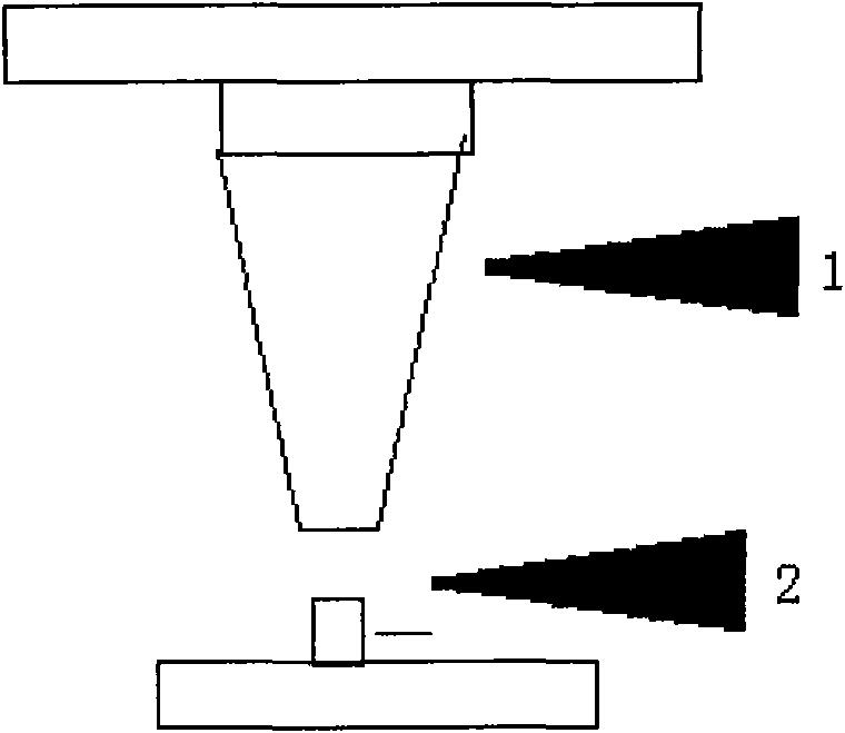
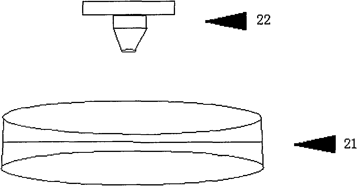
[0014] The fabrication method of the flip-chip light emitting diode chip of the present invention will be described in detail below with reference to the accompanying drawings.
[0015] The preparation method of light-emitting diode chip of the present invention comprises the following steps:
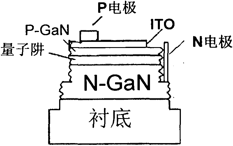
[0016] First, an array of light-emitting diode chips is grown on a wafer-shaped growth substrate by epitaxy, wherein each light-emitting diode chip includes a semiconductor substrate layer, an N-type semiconductor layer, a quantum well layer, a P-type semiconductor layer, and an N-type semiconductor layer. The structure formed by the N electrode on the upper layer and the P electrode on the P-type semiconductor layer can be a vertical structure, a front-chip structure or a flip-chip structure. Such as figure 2 As shown, it is a light-emitting diode chip with a positive structure, which includes a sapphire substrate layer, an N-GaN layer, a quantum well layer, a P-GaN layer, an N elect...
PUM
 Abstract
Description
Claims
Application Information


