
Large-power forward LED chip structure

A LED chip and high-power technology, applied in lighting devices, lighting device components, lighting device cooling/heating devices, etc. problem, to achieve the effect of improving light extraction efficiency, improving heat dissipation capacity, and realizing high power and high brightness

Inactive Publication Date: 2010-12-29
SHENZHEN CENTURY EPITECH LEDS
View PDF0 Cites 6 Cited by
  • Summary
  • Abstract
  • Description
  • Claims
  • Application Information

AI Technical Summary

Problems solved by technology

[0004] The purpose of the present invention is to provide a high-power front-mounted LED chip structure with high thermal conductivity and high light extraction efficiency for the problems of poor heat dissipation and low light extraction efficiency of high-power LEDs in the prior art.
[0006] Compared with the prior art, the high-power front-mounted LED chip of the present invention solves the heat dissipation and improves the light extraction efficiency encountered by high-power LED chips at high current densities by using a combination of heat-conducting base and DBR optical reflection film The problem of using this structure of the chip also has the following advantages:

Method used


Image

  • Large-power forward LED chip structure
  • Large-power forward LED chip structure
  • Large-power forward LED chip structure

Examples


Embodiment Construction

[0012] In order to make the technical problems, technical solutions and beneficial effects to be solved by the present invention clearer, the present invention will be further described in detail below in conjunction with the accompanying drawings and embodiments. It should be understood that the specific embodiments described here are only used to explain the present invention, not to limit the present invention.

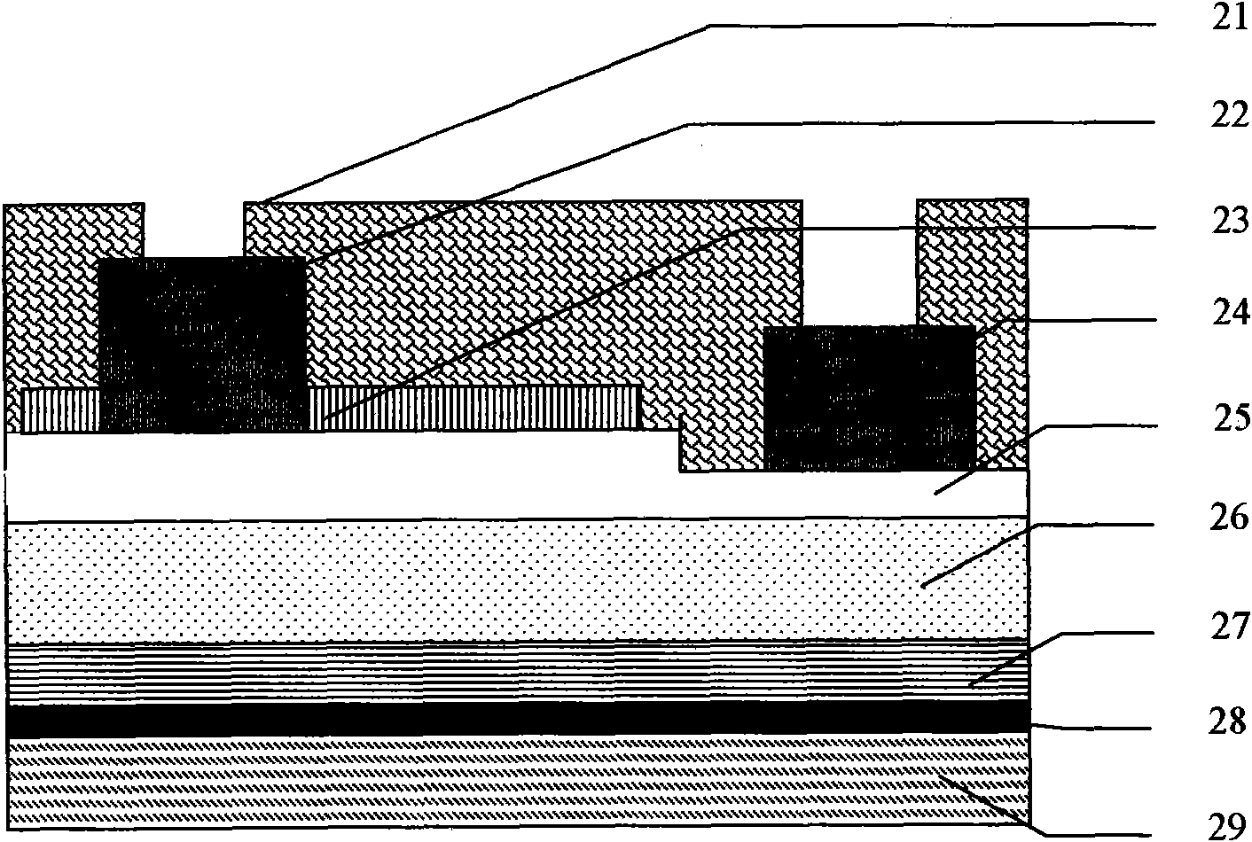
[0013] like figure 2 As shown, the present invention provides a high-power front-loading LED chip structure, including a transparent passivation layer 21, a P pressure pad 22, a transparent electrode layer 23, an N electrode 24, an LED epitaxial layer 25, a sapphire substrate 26, reflection and solder Layer 28, wherein: the surface of the reflective and solder layer 28 is formed with a DBR optical reflective layer 27 by means of optical coating, and a high thermal conductivity base layer 29 is provided at the bottom of the reflective and solder layer 28 .

[0014...


PUM

PropertyMeasurementUnit
Thicknessaaaaaaaaaa
Thicknessaaaaaaaaaa

Abstract

The invention relates to a large-power forward LED chip structure comprising a transparent passivating layer, a P pressure welding point, a transparent electrode layer, an N electrode, an LED epitaxial layer, a sapphire substrate and a reflection solder layer, wherein the surface of the reflection solder layer forms a DBR optical reflection layer in the mode of optical coating; and the bottom of the reflection solder layer is provided with a high heat conduction substrate layer. The large-power forward LED chip of the invention combines the heat conduction substrate with the DBR optical reflection film to solve the problem of heat dissipation and light emitting efficiency improvement for the large-power LED chip when high-current density is small.

Description

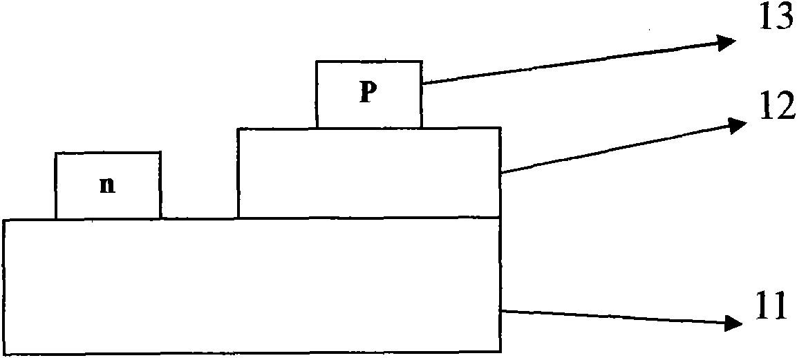
technical field [0001] The invention relates to the field of semiconductor devices, in particular to a high-power front-mounted LED chip structure with high heat conduction and high light extraction efficiency. Background technique [0002] At present, the basic structure of blue light, green light and other light-emitting diodes (LEDs) is to epitaxially grow InGaN / GaN light-emitting semiconductor materials on a sapphire substrate, and then make positive / negative electrodes on the upper surface of the epitaxial layer for injecting current so that it can transfer electric energy converted into light energy. As shown in Figure-1, it is a schematic cross-sectional structure diagram of a typical blue LED chip. The chip is mainly composed of three parts, a sapphire substrate 11, an epitaxial layer 12, and an ohmic electrode 13 (including two electrodes p and n), The positive ohmic electrode is made on the p-type GaN layer. In order to improve the uniformity of current injection...

Claims


Application Information

Patent Timeline
IPC IPC(8): F21S2/00F21V7/22F21V29/00H01L33/00F21Y101/02F21V29/503F21V29/70
Inventor 吴大可朱国雄张坤
Owner SHENZHEN CENTURY EPITECH LEDS
Learn More