Check patentability & draft patents in minutes with Patsnap Eureka AI!

Packaging structure

A technology of packaging structure and packaging area, applied in electrical components, electrical solid devices, circuits, etc., can solve the problems of lead frame collision, affecting the yield of semiconductor packaging process, etc.

Active Publication Date: 2010-12-29
CHIPMOS TECH INC
View PDF0 Cites 0 Cited by
  • Summary
  • Abstract
  • Description
  • Claims
  • Application Information

AI Technical Summary

Problems solved by technology

[0004] However, in the transportation process after sealing, the lead frame may be subjected to improper external force collision due to improper feeding or poor operation by personnel, or the edge part of the sealant may be peeled off from the lead frame due to thermal expansion and contraction, causing the entire package body to be damaged. Become a defective product, thereby affecting the process yield of semiconductor packaging

Method used


Image

  • Packaging structure
  • Packaging structure
  • Packaging structure

Examples


Embodiment Construction

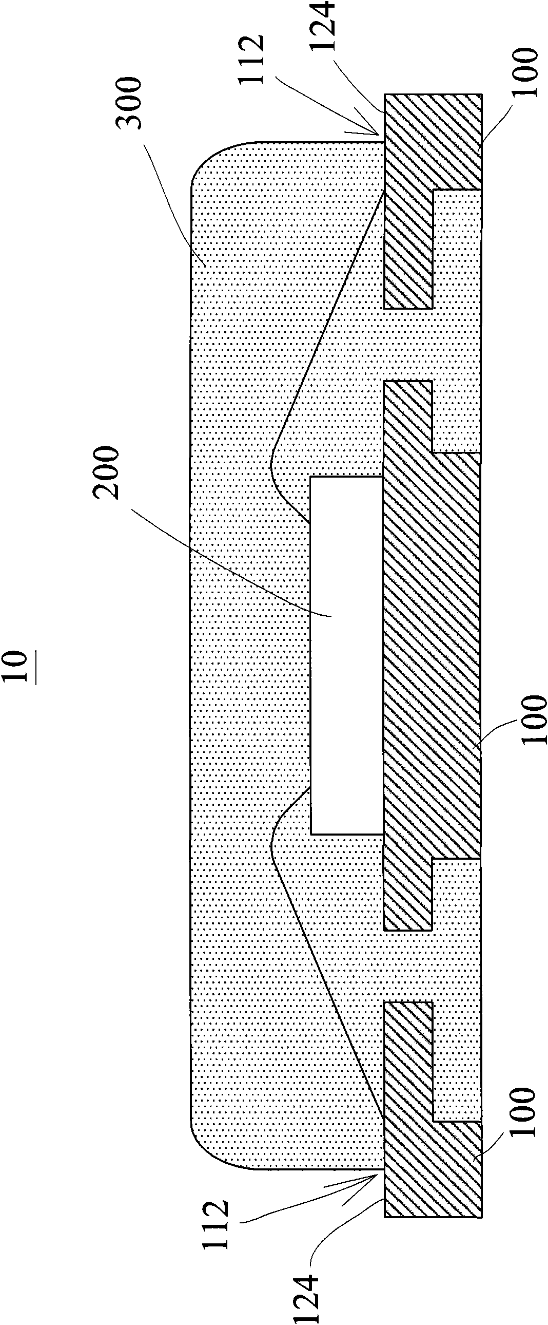
[0028] One embodiment of the present invention is a packaging structure 10 applied in a semiconductor packaging process. see figure 1 , which is a schematic partial cross-sectional view of a single package on the package structure 10 . The package includes: a lead frame 100 , a chip 200 and a molding compound 300 . As shown in the figure, the chip 200 is placed on the lead frame 100 and electrically connected to the lead frame 100 by bonding; in other implementations, the chip 200 can also be electrically connected to the lead frame 100 by other means. The molding compound 300 molds and covers the chip 200 on the lead frame 100 . In this embodiment, the lead frame 100 is applied to a Quad Flat No lead (QFN) package structure. In other implementations, those skilled in the art can easily deduce the application of other package structures. .

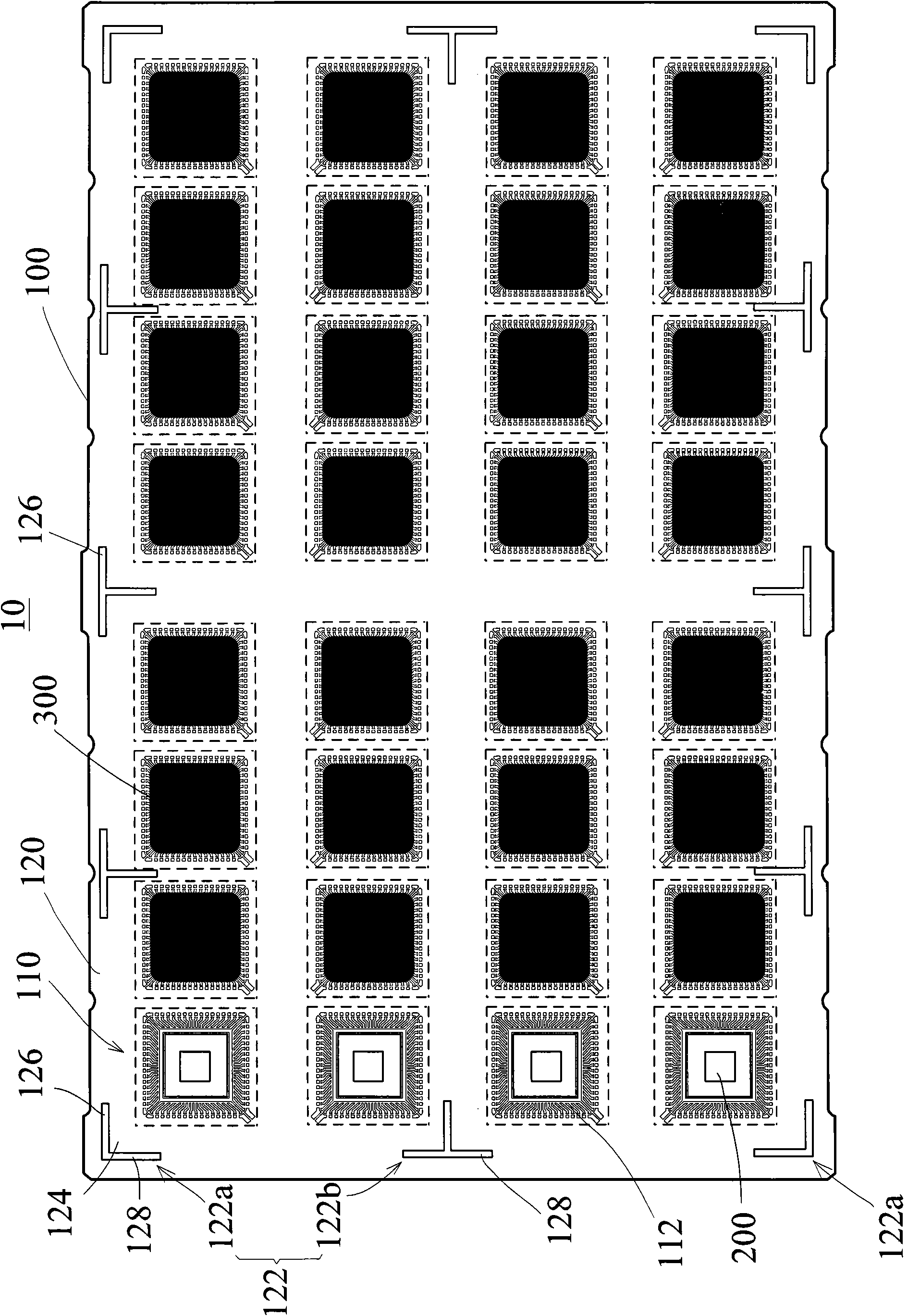
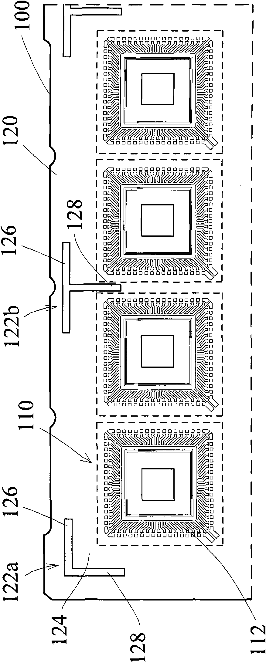
[0029] Please continue to refer to figure 2 and image 3 , the lead frame 100 of the package structure 10 has a plurality of packa...


PUM


Abstract

The invention provides a packaging structure which comprises a lead frame, at least one chip and at least one moulding material, wherein the lead frame is provided with at least one packaging area unit and a lead frame border; the at least one packaging area unit has a moulding and sealing range; the lead frame border surrounds the at least one packaging area unit and has at least one hollow structure; the at least one hollow structure is formed at the external edge outside the moulding and sealing range, comprises a first direction cavity and a second direction cavity and respectively extends along both side edges of the moulding and sealing range of the at least one packaging area unit; and the at least one moulding material is used for moulding and sealing the at least one chip in the moulding and sealing range of the at least one packaging area unit of the lead frame.

Description

technical field [0001] The invention relates to a packaging structure, in particular to a packaging structure used in semiconductor technology. Background technique [0002] Wafer manufacturing plants extract silicon crystal rods, and after the silicon crystal rods are ground, polished and cut, the raw materials for the semiconductor process can be obtained: wafers. Chips are produced by semiconductor processing procedures such as deposition, etching, coating, and development, and then sent to semiconductor packaging factories to package integrated circuit chips, which are then sold to computer or mobile phone manufacturers to produce various products. [0003] The semiconductor packaging process includes wafer cutting, die bonding, wire bonding, glue sealing, printing, etc. In the above process, in addition to the wafer cutting step, there must be a carrier to help carry the chips obtained after wafer cutting, and then complete the process such as bonding. Substrates (rigi...

Claims


Application Information

Patent Timeline
Patent Type & Authority Applications(China)
IPC IPC(8): H01L23/495H01L23/13
CPCH01L2224/48247H01L2224/48091H01L2924/181
Inventor 杜武昌侯博凯
Owner CHIPMOS TECH INC
Features
  • R&D
  • Intellectual Property
  • Life Sciences
  • Materials
  • Tech Scout
  • Unparalleled Data Quality
  • Higher Quality Content
  • 60% Fewer Hallucinations
Learn More