New compound semiconductor and producing method thereof, and solar cell and thermoelectric conversion element using the same
A technology of solar cells and thermoelectric conversion, applied in the direction of oxide conductors, sulfide conductors, semiconductor devices, etc.
- Summary
- Abstract
- Description
- Claims
- Application Information
AI Technical Summary
Problems solved by technology
Method used
Image

Examples
Embodiment 1
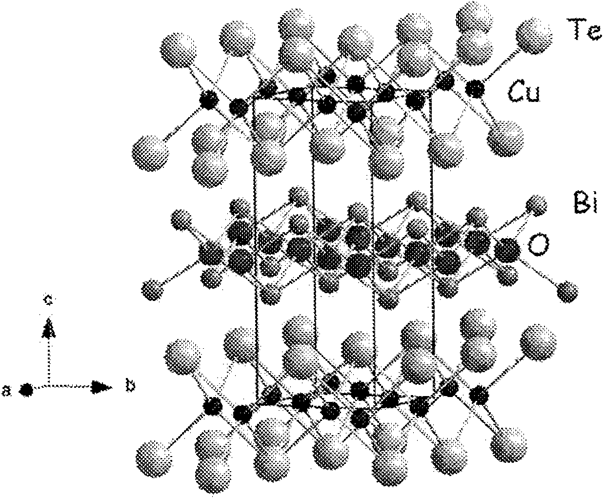
[0068] BiCuOTe
[0069] To prepare BiCuOTe, 1.1198 g of Bi 2 o 3 (Aldrich, 99.9%, 100 mesh), 0.5022g of Bi (Aldrich, 99.99%, <10m), 0.4581g of Cu (Aldrich, 99.7%, 3m) and 0.9199g of Te (Aldrich, 99.99%, about 100 mesh ), and then heated in a vacuum quartz tube at 510 °C for 15 hours to obtain BiCuOTe powder.
[0070] Cu X-ray tube ( 50kV, 40mA) to measure powder X-ray diffraction (XRD) data. The step size is 0.02 degrees.
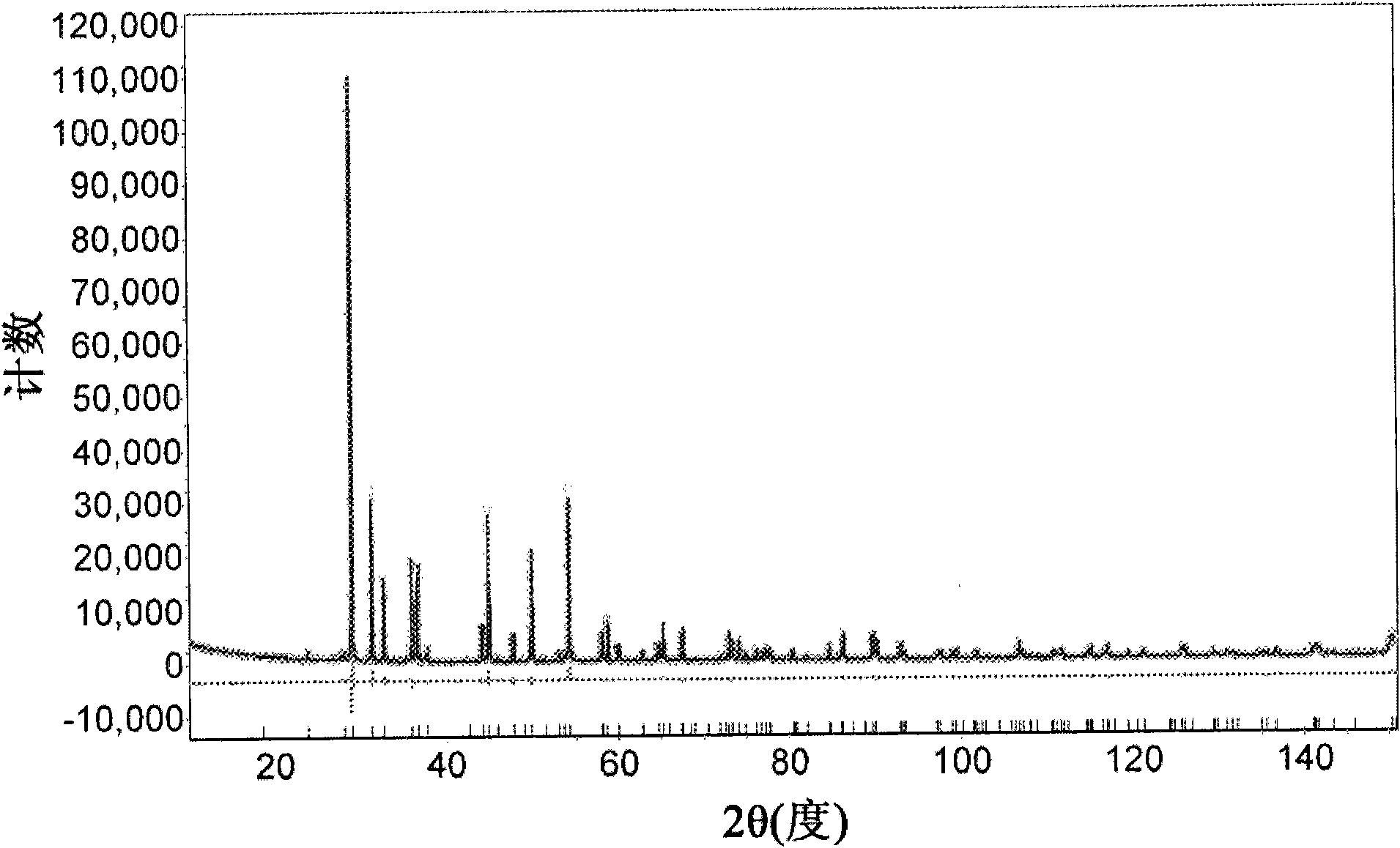
[0071] The TOPAS program (R.W. Cheary, A. Coelho, J. Appl. Crystallogr. 25 (1992) 109-121; Bruker AXS, TOPAS 3, Karlsruhe, Germany (2000)) was used to determine the crystal structure of the obtained material. The analysis results are shown in Table 1 and figure 2 middle.
[0072] 【Table 1】
[0073] atom
Location
x
y
z
share
Beq
Bi
2c
0.25
0.25
0.37257(5)
1
0.56(1)
Cu
2a
0.75
0.25
0
1
0.98(3)
O
2b
0.75
0.25
0....
Embodiment 2
[0078] BiCu 0.9 OTe
[0079] In order to prepare BiCu 0.9 OTe, 1.1371 g of Bi was thoroughly mixed by using an agate mortar 2 o 3 (Aldrich, 99.9%, 100 mesh), 0.51g of Bi (Aldrich, 99.99%, 0.9 OTe powder.
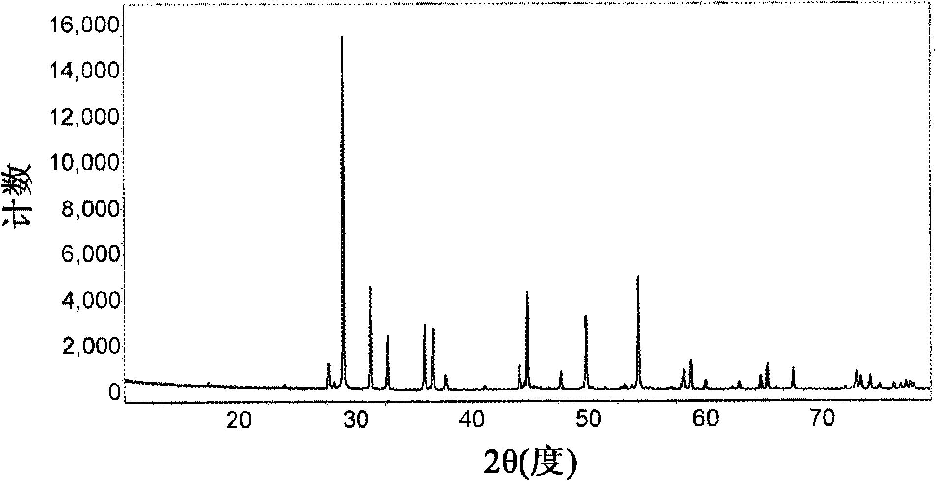
[0080] X-ray diffraction analysis of this sample was carried out in the same manner as in Example 1. like image 3 As shown, the material obtained in Example 2 was identified as BiCu 0.9 TeO.
Embodiment 3
[0082] Bi 0.98 Pb 0.02 CuOTe
[0083] To prepare Bi 0.98 Pb 0.02 CuOTe, by thoroughly mixing 2.5356 g of Bi using an agate mortar 2 o 3 (Aldrich, 99.9%, 100 mesh), 1.1724g of Bi (Aldrich, 99.99%, 0.98 Pb 0.02 CuOTe powder.
[0084] Cu X-ray tube ( 50kV, 40mA) to measure powder X-ray diffraction (XRD) data. The step size is 0.02 degrees.
[0085] The TOPAS program (R.W. Cheary, A. Coelho, J. Appl. Crystallogr. 25 (1992) 109-121; Bruker AXS, TOPAS 3, Karlsruhe, Germany (2000)) was used to determine the crystal structure of the obtained material. The analysis results are shown in Table 2 and Figure 5 middle.
[0086] 【Table 2】
[0087] atom
Location
x
y
z
share
Beq
Bi
2c
0.25
0.25
0.37225(12)
0.98
0.59(4)
Pb
2c
0.25
0.25
0.37225(12)
0.02
0.59(4)
Cu
2a
0.75
0.25
0
1
1.29(10)
O
2b
0.75
0.25...
PUM
| Property | Measurement | Unit |
|---|---|---|
| diameter | aaaaa | aaaaa |
| length | aaaaa | aaaaa |
| thickness | aaaaa | aaaaa |
Abstract
Description
Claims
Application Information