Method for manufacturing microwave power device by using double level polysilicon device structure

A polysilicon device, microwave power technology, applied in semiconductor/solid-state device manufacturing, electrical components, circuits, etc., can solve problems such as higher power output of unfavorable devices, large extrinsic base area, and device reliability discounts. The effect of improving power output characteristics, avoiding registration deviation, and reducing parasitic capacitance and parasitic resistance components

Inactive Publication Date: 2011-01-19
WUXI JINGKAI TECH
View PDF2 Cites 6 Cited by
  • Summary
  • Abstract
  • Description
  • Claims
  • Application Information

AI Technical Summary

Problems solved by technology

The manufacture of traditional silicon bipolar microwave high-power transistors has always followed the conventional non-self-aligned planar bipolar transistor structure, but for this conventional planar structure, there are the following disadvantages: emitter and emitter, base The electrode and the base are in direct contact; the isolation of the base and emitter is still completely achieved by photolithographic patterns
When the number of emitters increases, because it is difficult to accurately control the self-aligned vertical evaporation to form the metal contact between the base and the emitter, the device is prone to short circuit, and the reliability of the device is greatly reduced.
Secondly, the base lead is opened in the active area, and the extrinsic base area of ​​the device is relatively large, which is another important reason that is not conducive to the device to obtain greater power output

Method used


Image

  • Method for manufacturing microwave power device by using double level polysilicon device structure
  • Method for manufacturing microwave power device by using double level polysilicon device structure
  • Method for manufacturing microwave power device by using double level polysilicon device structure

Examples


Embodiment Construction

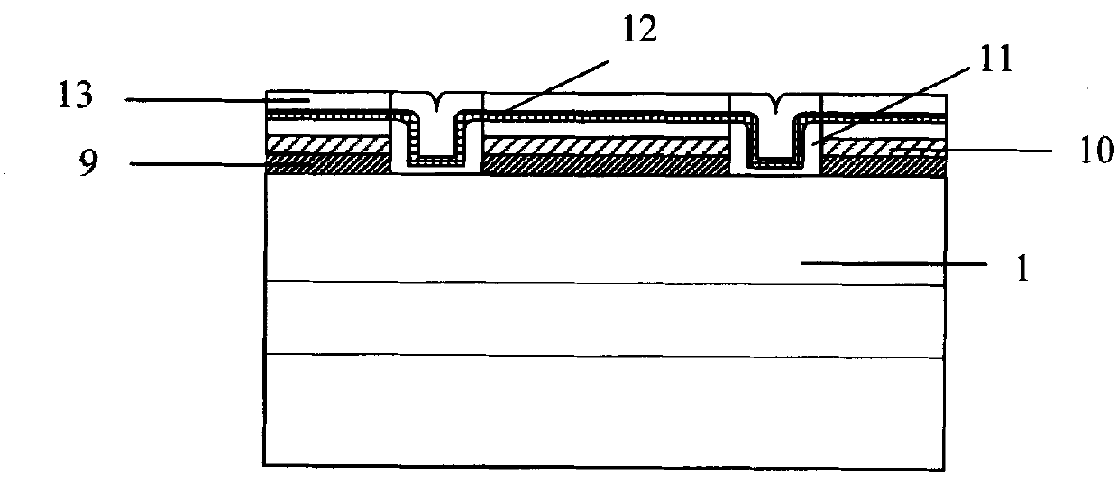
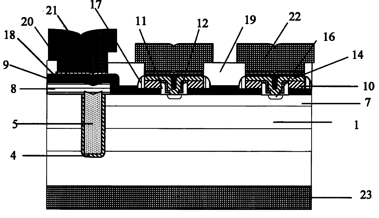
[0039] The method for preparing a microwave power device with a double-layer polysilicon emitter structure of the present invention will be described in detail below in conjunction with the accompanying drawings:

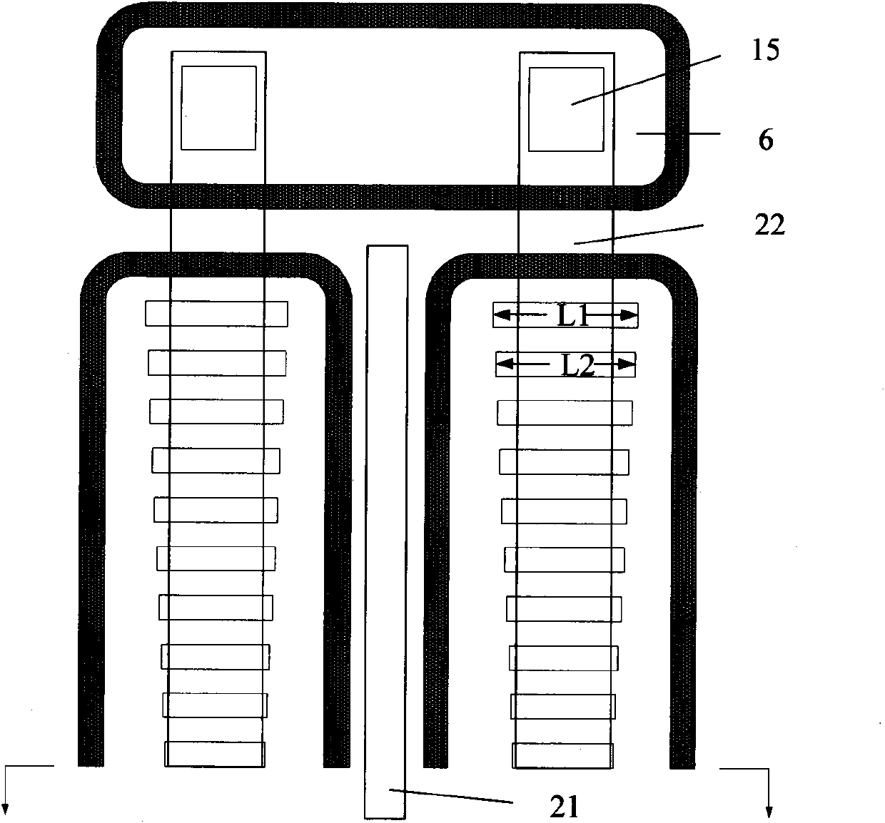
[0040] Such as figure 1 As shown, the present invention utilizes self-alignment technology to prepare a microwave power device with a double-layer polycrystalline silicon device structure. After the process, the insulating oxide layer 4 is thermally grown, undoped polysilicon 5 is deposited and planarized to form a deep trench isolation structure; the area surrounded by the deep trench is implanted with boron ions to obtain the implanted area 6 and the series ballast resistance of the device. Active base region 7, P-type doped polysilicon 9 and dielectric isolation layer 10 are successively placed on the active base region 7 and field oxygen 8, and the dielectric isolation layer 10 is anisotropically etched by plasma etching RIE and ICP and other equipment respectiv...


PUM


Abstract

The invention discloses a method for manufacturing a microwave power device by using a double level polysilicon device structure. The method of the invention adopts a deep groove isolation technique and inhomogeneous thermal design, realizes the acinaceous cellular structure, adopts outer base region composite plate to carry out photoetching, vertically etches a monox dielectric layer and outer base polycrystalline silicon to obtain the outer base region window of the ratio change of the length and the like, and forms a compound L-shaped side wall capable of adjusting the length of an emitting electrode by means of autocollimation in the outer base region window. In the invention, the emitting electrode polycrystalline silicon composite plate is adopted to carry out photoetching, the emitting electrode polycrystalline silicon and the dielectric layer are vertically etched by utilizing autocollimation, the selective side wall protection technology is combined, under the scale of the deep submicron, and the polycrystalline silicon refractory metallic silicide with low film resistivity is realized by means of autocollimation, thereby avoiding the short circuit connection of two types of polycrystalline silicon leads, reducing the restriction of parasitic components of the interconnected leads on improving the characters of the microwave power device under the graph scale of submicron and deep submicron, thereby improving the overall performance of the microwave power device and the microwave performance thereof.

Description

technical field [0001] The invention belongs to a method for preparing a power semiconductor device, in particular to a method for preparing a microwave power device by self-alignment of a double-layer polysilicon device structure. Background technique [0002] Because of its high output power and good reliability, silicon microwave pulse power transistors have become the key components of navigation equipment and phased array radars below the S-band. The manufacture of traditional silicon bipolar microwave high-power transistors has always followed the conventional non-self-aligned planar bipolar transistor structure, but for this conventional planar structure, there are the following disadvantages: emitter and emitter, base The pole electrode is in direct contact with the base region; the isolation of the base and emitter is still completely achieved by photolithographic patterns. This actually invisibly increases the area of ​​the device and increases the parasitic base ...

Claims


Application Information

Patent Timeline
Patent Type & Authority Applications(China)
IPC IPC(8): H01L21/331H01L21/762H01L21/768
Inventor 黄伟徐湘海王胜万清胡南中
Owner WUXI JINGKAI TECH
Why Eureka
Try Eureka