Super Junction VDMOS device

A device and electrode technology, which is applied in the field of Super Junction VDMOS devices and power semiconductor devices, can solve the problems of increasing device manufacturing costs, device leakage current, and device on-resistance, and achieve improved heat dissipation performance, small device size, and reduced The effect of device contact resistance

Inactive Publication Date: 2011-01-19
UNIV OF ELECTRONICS SCI & TECH OF CHINA
View PDF5 Cites 39 Cited by
  • Summary
  • Abstract
  • Description
  • Claims
  • Application Information

AI Technical Summary

Problems solved by technology

However, due to the introduction of the Schottky contact structure 11, the leakage current of the device increases, and because the Schottky contact changes the original gate structure, the multiple electrons formed on the surface of the N-region epitaxial layer when the original positive gate bias is applied layer no longer exists, making the device on-resistance increase
To improve these shortcomings, a better process line width is required, which increases the manufacturing cost of the device

Method used


Image

  • Super Junction VDMOS device
  • Super Junction VDMOS device
  • Super Junction VDMOS device

Examples


Embodiment Construction

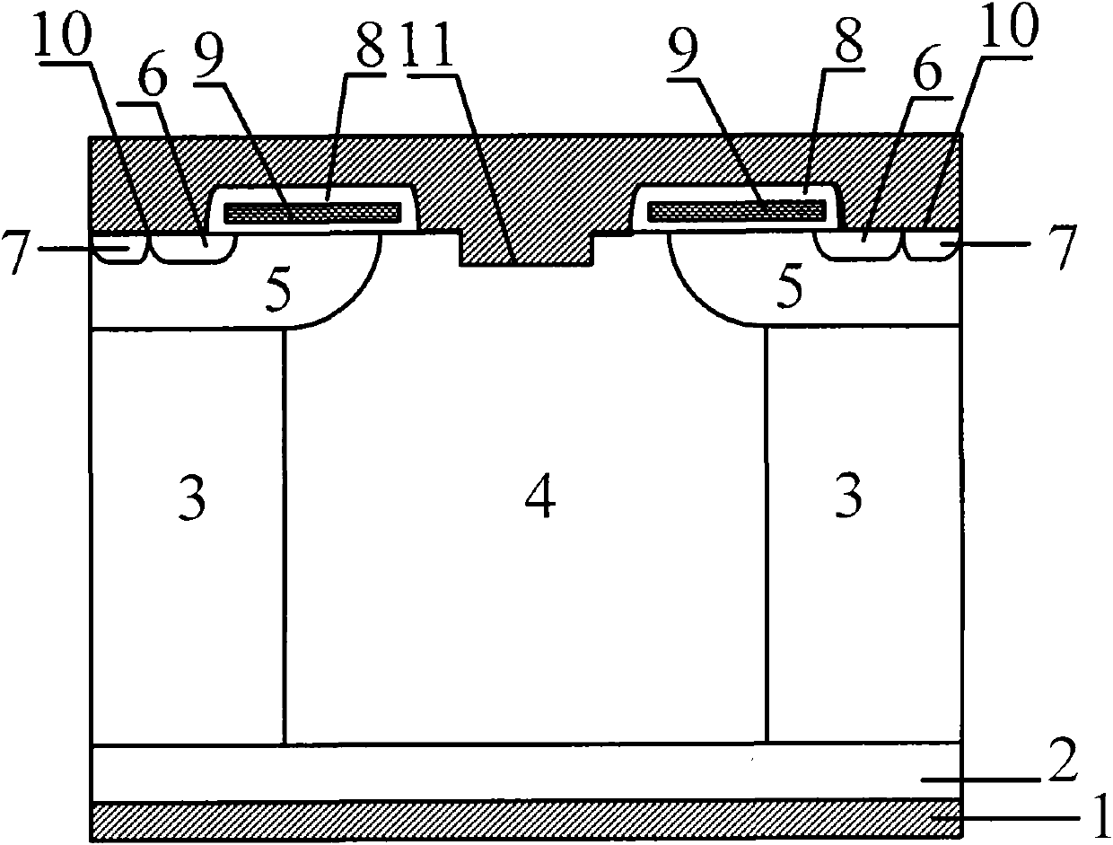
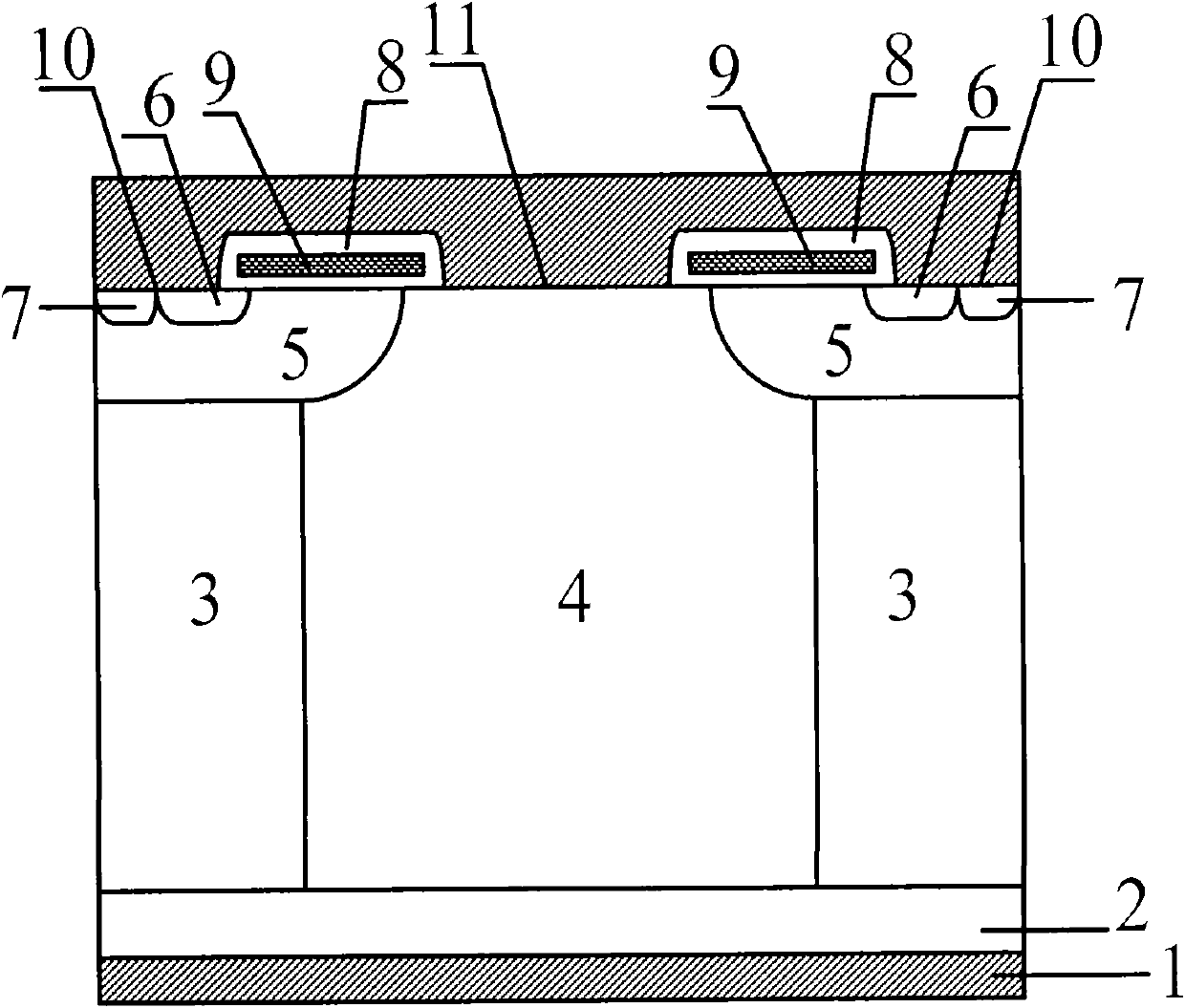
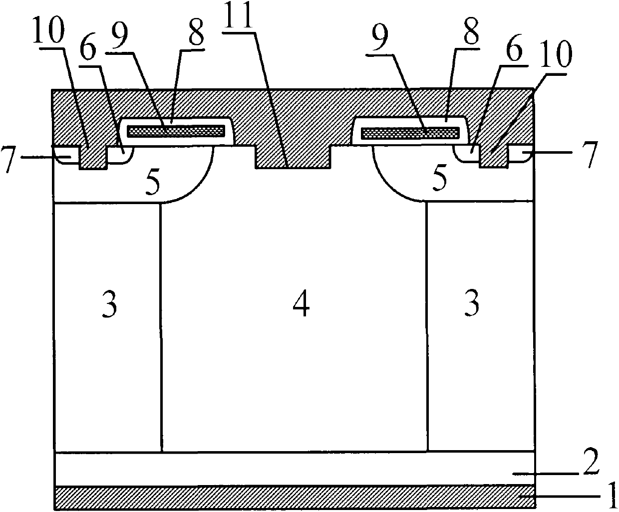
[0023] A Super Junction VDMOS device, such as image 3 shown, including N + Substrate 2, located at N + The metal drain 1 on the back surface of the substrate 2 is located at N + The Super Junction structure on the surface of the substrate 2 , the polysilicon gate electrode 9 and the metal source electrode 10 . The Super Junction structure is formed by sandwiching an N-type column area 4 between two P-type column areas 3 . There is a P-type base region 5 on both sides of the top of the Super Junction structure, and the P-type base region 5 is in contact with the P-type column region 3 and the N-type column region 4 respectively; the two P-type base regions 5 have N + source region 6 and P + body area 7. The polysilicon gate electrode 9 is located above the P-type base region 5 and the N-type pillar region 4 , and is insulated from the P-type base region 5 and the N-type pillar region 4 by a gate oxide layer. The metal source electrode 10 is located on the uppermost layer...


PUM


Abstract

The invention discloses a Super Junction VDMOS device, which belongs to the technical field of semiconductor power devices. In the invention, a trench Schottky contact structure is introduced on the basis of the Super Junction VDMOS device with a flat Schottky contact structure. The trench Schottky contact structure is that: a polycrystalline gate electrode is divided into two sections above an N-type pillar area; meanwhile, the area, which is between the two sections of the polycrystalline gate electrode, of a metal source electrode is extended downward to the N-type pillar area and forms the trench Schottky contact structure on the surface contacted with the N-type pillar area. In addition, the two ends of the metal source electrode may have a trench ohmic contact structure. The Super Junction VDMOS device provided by the invention has an excellent reverse recovery property; with a requirement of the same reverse recovery property, the requirement on the wide of a process line in the preparation of the device is lowered, and the size of the element is smaller; and the trench ohmic contact structure can reduce the contact resistance of the device and improve the radiation performance of the device. The two trench structure can use the same mask plate, and thus, the manufacturing cost of the device does not increase obviously.

Description

technical field [0001] The invention belongs to the technical field of electronics, relates to a power semiconductor device, in particular to a Super Junction VDMOS device. Background technique [0002] Super Junction VDMOS is a new type of power semiconductor device that develops rapidly and is widely used. It is based on ordinary vertical double diffused metal oxide semiconductor (VDMOS), by introducing SJ (Super Junction) structure, in addition to VDMOS high input impedance, fast switching speed, high operating frequency, voltage control, good thermal stability, In addition to the characteristics of simple driving circuit and easy integration, it also overcomes the disadvantage that the on-resistance of VDMOS increases with the breakdown voltage to the power of 2.5. At present, Super Junction VDMOS has been widely used in power supplies or adapters for consumer electronics products such as personal computers, notebook computers, netbooks or mobile phones, lighting (high-...

Claims


Application Information

Patent Timeline
Patent Type & Authority Applications(China)
IPC IPC(8): H01L29/78H01L29/06H01L29/417H01L29/47
Inventor 李泽宏胡涛邓光平钱振华洪辛张波
Owner UNIV OF ELECTRONICS SCI & TECH OF CHINA
Why Eureka
Try Eureka