
Fabrication method of rectifier diode

A technology of rectifying diodes and manufacturing methods, which is applied in semiconductor/solid-state device manufacturing, electrical components, circuits, etc., can solve the problems of inability to achieve optimal distribution of minority carrier lifetime, reduce minority carrier lifetime, and large on-state voltage drop, and achieve improved blocking Volt-ampere characteristics and current density, improved reliability, and small on-state voltage drop

Active Publication Date: 2015-07-22
鞍山市华辰电力器件有限公司
View PDF3 Cites 0 Cited by
  • Summary
  • Abstract
  • Description
  • Claims
  • Application Information

AI Technical Summary

Problems solved by technology

The device manufactured by paper source + independent platinum diffusion method has the disadvantage of large on-state pressure drop, and the gas generated during diffusion will pollute the environment; while the device manufactured by diffusion of phosphorus oxychloride and boron trioxide as impurity source The concentration distribution is uniform and the inversion is serious, resulting in the phenomenon of the same polarity of the cathode and the anode
If the reverse recovery time needs to be shortened, electron irradiation or platinum expansion is required. Both methods reduce the minority carrier lifetime uniformly, but cannot achieve the optimal distribution of the minority carrier lifetime.

Method used

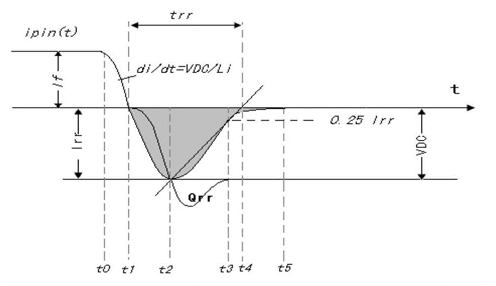
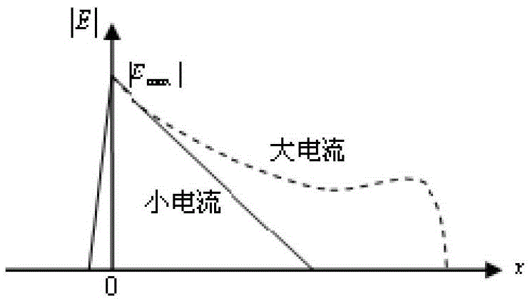
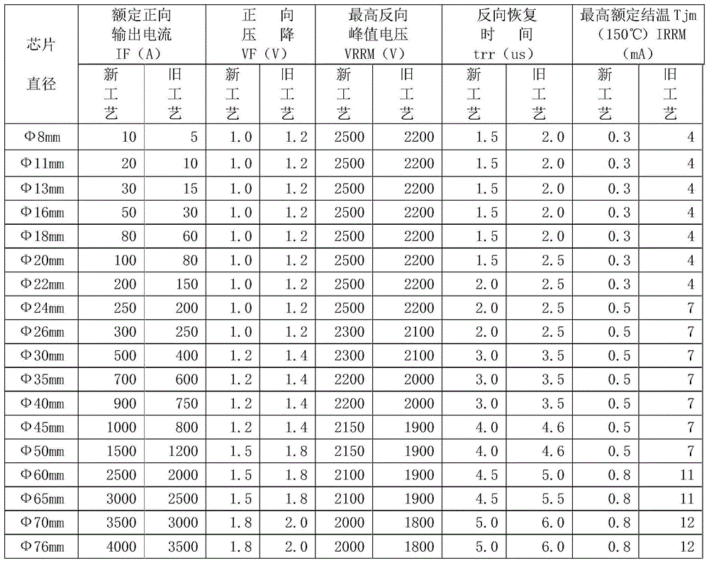

Image

  • Fabrication method of rectifier diode
  • Fabrication method of rectifier diode
  • Fabrication method of rectifier diode

Examples


Embodiment Construction

[0027] The present invention will be further described below in conjunction with specific embodiment:

[0028] The invention discloses a manufacturing method of sub-dense sub-dense rectifier diodes, which comprises supersanding of silicon wafers, cleaning of silicon wafers, cleaning of quartz frames and quartz ingots, diffusion, detection, and manufacturing steps of diffusion sources. Phosphorus, boron, and platinum liquid sources are used once. The full diffusion process makes the surface concentration distribution uniform, and realizes the optimal distribution of minority carrier lifetime through the absorption of phosphosilicate glass. The specific operation steps are as follows:

[0029] 1) Silicon wafer super sand

[0030] Place the silicon wafer on a high-temperature PTFE frame, put it into the cleaning solution, the ratio of the cleaning solution is, electronic cleaning solution: deionized water = 2.7ml: 1000ml, ultrasonic cleaning for 30 to 40 minutes, and then use 60 ...


PUM


Abstract

The invention relates to the field of a diode production technology, in particular to a fabrication method of a rectifier diode. The method comprises the steps of silicon wafer ultrasonic sanding, silicon wafer cleaning, quartz frame and quartz lead cleaning, diffusion, detection and diffusion source fabrication. The method is characterized in that a primary perfect diffusion technology of liquid phosphorus, boron and platinum sources is adopted, the optimization distribution of the minority carrier lifetime is realized with the absorption of phosphorosilicate glass, the open pipe diffusion is adopted, the temperature of a diffusion furnace is 1249-1251 DEG C, the diffusion time is 12-15h, the phosphorus source, the boron source and platinum micropowder are placed in, and a P-type area requires that R P=1.1-1.3R / ohm and XjP=87-93 micrometers. Compared with the prior art, the method has the benefits that 1), the uniformity of surface concentration of a silicon wafer is improved and 20-22h is shortened compared with a paper source diffusion technology, and 2), the service life is increased by about 1500h compared with a common diode.

Description

technical field [0001] The invention belongs to the field of diode production technology, and in particular relates to a method for manufacturing a rectifier diode. Background technique [0002] At present, in the production process of rectifier diodes in China, "N" type single crystal silicon is used as raw material to prepare PN junction. There are two common methods, namely, paper source + independent platinum diffusion method and phosphorus oxychloride and boron trioxide Diffusion method. The device manufactured by paper source + independent platinum diffusion method has the disadvantage of large on-state pressure drop, and the gas generated during diffusion will pollute the environment; while the device manufactured by diffusion of phosphorus oxychloride and boron trioxide as impurity source The concentration distribution is uniform, and the inversion is serious, resulting in the same polarity of the cathode and the anode. If the reverse recovery time needs to be shor...

Claims


Application Information

Patent Timeline
Patent Type & Authority Patents(China)
IPC IPC(8): H01L21/329
Inventor 于能斌王景波刘欣宇
Owner 鞍山市华辰电力器件有限公司
Learn More