
Electronic tag antenna

A technology of electronic tags and dipole antennas, applied in the fields of electronic tag antennas and radio frequency identification, can solve the problems of impedance adjustability limitation, failure to meet matching requirements, and failure to meet ASIC impedance matching requirements, etc., to achieve simple structure and characteristic impedance Flexible and adjustable effects

Inactive Publication Date: 2011-01-19
UNIV OF ELECTRONICS SCI & TECH OF CHINA
View PDF4 Cites 10 Cited by
  • Summary
  • Abstract
  • Description
  • Claims
  • Application Information

AI Technical Summary

Problems solved by technology

[0005] figure 1 It is an ordinary dipole antenna. This type of antenna has a specific length for a specific operating frequency, and its impedance is relatively fixed, but it cannot meet the variable ASIC impedance matching requirements; figure 2 In order to simply fold the dipole antenna, this type of antenna can partially make up for the lack of antenna impedance adjustability, but when the bending distance of the antenna is limited, the reactance component of the impedance usually presents capacitive in the UHF frequency band, which cannot satisfy most Matching requirements of ASIC chips; image 3 It is a dipole antenna with ring-shaped stubs loaded in the middle. The ring-shaped stubs loaded by this type of antenna are inductive to the center-balanced feed dipole, but the overall length of the antenna is too long. When the bending distance is limited, the impedance adjustability will also be affected. limit

Method used


Image

  • Electronic tag antenna
  • Electronic tag antenna
  • Electronic tag antenna

Examples


Embodiment 1

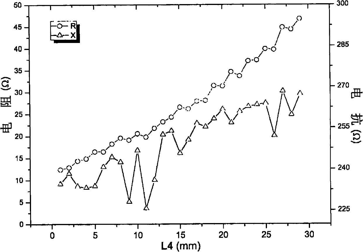
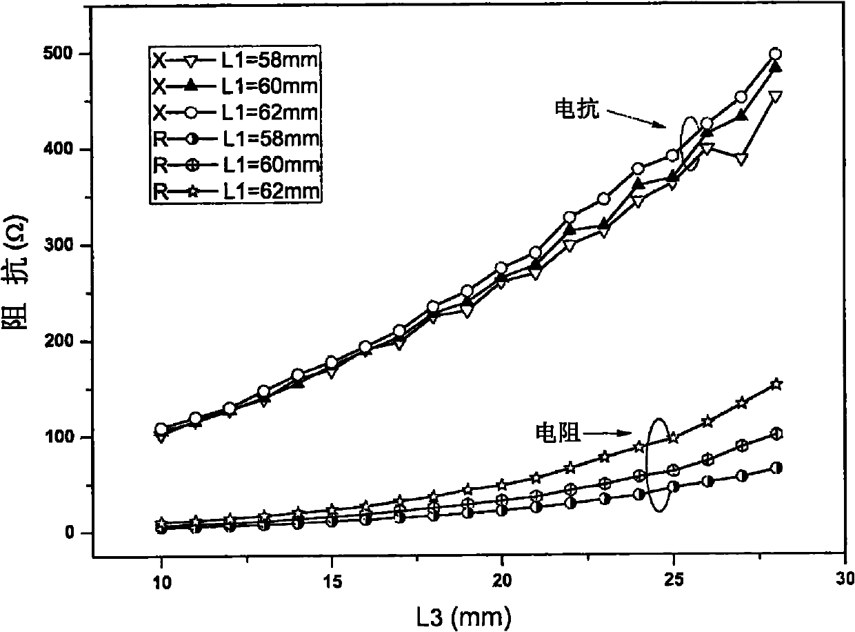
[0027] Taking the Monza2 chip of Impinj Company as an example, the design frequency is 910MHz, and the test value of the chip impedance is 33.45-j246.61Ω, and the antenna is designed. Through optimization, when the size of the antenna is L1=61 mm, L2=33 mm, L3=19 mm, L4=20 mm, and the line width of the dipole antenna and all stubs is 1 mm and the vertical distance of all loaded stubs When equal to 1 mm, the antenna impedance Z 0 =33.61+j248.42Ω, which can achieve a good match with the ASIC chip, the reflection coefficient reaches -38dB, and the gain of the antenna reaches 2.41dB.

Embodiment 2

[0029] Also take Impinj's Monza2 chip as an example, take the design frequency of 2.45GHz, and design the antenna for the same impedance. The optimization is obtained, when the size of the antenna is L1=19.3 mm, L2=6.9 mm, L3=6.8 mm, L4=10 mm, and the line width of the dipole antenna and all stubs is 1 mm and the vertical distance of all loaded stubs When equal to 1 mm, the antenna impedance Z 0 =33.45+j250.8Ω, which can achieve a good match with the ASIC chip, the reflection coefficient reaches -32dB, and the gain of the antenna reaches 2.38dB.


PUM

PropertyMeasurementUnit
Reflection coefficientaaaaaaaaaa

Abstract

The invention provides an electronic tag antenna suitable for ISO18000-6 / B / C and EPC GEN2 electronic tag standards and with high length-width ratio dimension property. Based on the conventional dipole antenna, branches of three types are loaded in the antenna, namely 1) an L-shaped bent branch is loaded at two ends respectively, 2) a loop branch is loaded on two sides of a middle feed point respectively, and 3) a vertical branch (22) is loaded between the middle feed point and the two ends respectively. By loading the three branches, high length-width ratio of the antenna can be achieved under the condition of meeting high antenna gain; and meanwhile, the real part and the virtual part of antenna impedance can be independently adjusted by changing the dimension of individual branches so that the impedance of different RFID chips can be adapted. The electronic tag antenna has a simple structure, flexible and adjustable characteristic impedance and high length-width ratio, and is suitable to be used in an environment with special limitation on the dimension of a tag; after dimension adjustment, the antenna structure can be used for UHF frequency range or microwave frequency range, and achieves good match with chips of numerous ASIC manufacturers at home and abroad.

Description

technical field [0001] The invention belongs to the technical field of antennas and relates to radio frequency identification (RFID) technology, in particular to an electronic tag antenna suitable for ISO18000-6 / B / C and EPC GEN2 electronic tag standards and having high aspect ratio size characteristics. Background technique [0002] Radio Frequency Identification (RFID) technology is a technology that uses radio frequency to automatically identify targets and obtain relevant data through non-contact two-way communication. It is currently one of the most popular intelligent identification technologies. A typical RFID system mainly includes three parts: the tag, the reader and the host control system. Among them, the performance of the tag plays an important role in the entire RFID system, accounting for more than 65% of the cost. The antenna design, which is an important part of the tag, is particularly important. important. [0003] Different from ordinary resonant antennas...

Claims


Application Information

Patent Timeline
IPC IPC(8): H01Q1/36H01Q9/16
Inventor 吕洪光邓腾彬王鲁豫王宇宋莉萍郑开明
Owner UNIV OF ELECTRONICS SCI & TECH OF CHINA
Learn More