Eureka AIR delivers breakthrough ideas for toughest innovation challenges, trusted by R&D personnel around the world.

LCD panel and manufacturing method thereof

A technology for a liquid crystal display panel and a manufacturing method, which is applied in nonlinear optics, instruments, optics, etc., can solve the problems of unstable product quality and display characteristics of liquid crystal display panels, liquid crystal pollution, etc., to reduce the probability of pollution and slow down the diffusion speed. , the effect of improving stability

Active Publication Date: 2012-04-04
BOE TECH GRP CO LTD +1
View PDF0 Cites 0 Cited by
  • Summary
  • Abstract
  • Description
  • Claims
  • Application Information

AI Technical Summary

Problems solved by technology

[0004] In the process of realizing the present invention, the inventor found that the technical scheme of setting the barrier frame with a thickness slightly greater than or equal to the thickness of the liquid crystal cell in the peripheral area of ​​the liquid crystal display panel in the prior art, although the incompletely cured seal in the cell-to-cell process of the liquid crystal display panel has been reduced. The frame glue may cause pollution to the liquid crystal, but there is a possibility that the total amount of liquid crystal in the display area may change before the liquid crystal cell of the liquid crystal display panel is deformed and after the deformation is restored, resulting in poor product quality and display characteristics of the liquid crystal display panel. Stable Technical Defects

Method used


Image

  • LCD panel and manufacturing method thereof
  • LCD panel and manufacturing method thereof
  • LCD panel and manufacturing method thereof

Examples


Embodiment 1

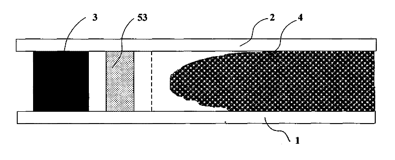
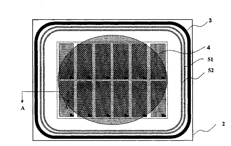
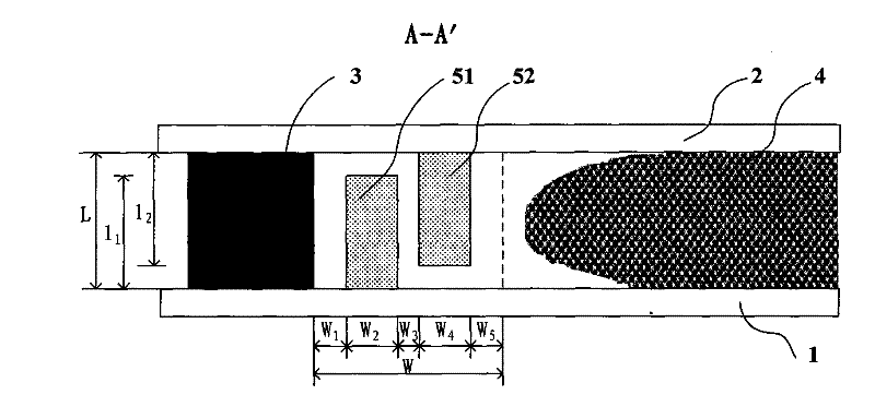
[0028] figure 2 The top view of the liquid crystal display panel during the liquid crystal diffusion process provided by the first embodiment of the present invention; image 3 for figure 2 A-A' sectional view of the liquid crystal display panel shown. Such as figure 2 with image 3 As shown, the liquid crystal display panel of this embodiment includes an array substrate 1 and a CF substrate 2, and the CF substrate 2 and the array substrate 1 are arranged opposite to each other up and down, wherein the display area of ​​the CF substrate 2 (the area indicated by the dotted line in the figure) and the array substrate 1 corresponds to the display area, and the peripheral area of ​​the CF substrate 2 (ie, the non-display area) corresponds to the peripheral area of ​​the array substrate 1 . The area between the display area of ​​the CF substrate 2 and the display area of ​​the array substrate 1 is a liquid crystal filling area, and liquid crystal 4 is filled in the liquid cr...

Embodiment 2

[0042] Figure 4 The top view of the liquid crystal display panel during the liquid crystal diffusion process provided by the second embodiment of the present invention; Figure 5 for Figure 4 B-B' sectional view of the liquid crystal display panel shown. Such as Figure 4 with Figure 5 As shown, the difference from Embodiment 1 of the present invention is that in this embodiment, two first barrier layers 51 are formed on the peripheral region of the array substrate 1 , and two second barrier layers 52 are formed on the peripheral region of the CF substrate 2 . The first barrier layers 51 and the second barrier layers 52 are arranged in parallel, alternately and at equal intervals. Figure 4 with Figure 5 Only the liquid crystal distribution during the liquid crystal diffusion process is shown, and those skilled in the art can understand that after the liquid crystal diffusion is completed, between the second barrier layer 52 and the array substrate 1, between the firs...

Embodiment 3

[0046] Image 6 It is a top view of the liquid crystal display panel provided by the third embodiment of the present invention. Such as Image 6 As shown, the difference from Embodiment 1 of the present invention is that the cross-sectional shape of the first barrier layer 51 and the second barrier layer 52 in this embodiment is a rounded rectangle, and a conduction peripheral area and a conductive peripheral area are formed at the rounded corners of the rounded rectangle. Opening 7 in the display area.

[0047] In the process of implementing the embodiment of the present invention, the inventors found that during the process of aligning liquid crystal display panels, due to the internal tension of the liquid crystal, the trajectory of the liquid crystal 4 spreading from the central part of the display area to the surroundings usually appears as an ellipse, and it can be seen that the liquid crystal 4 4 The probability that the liquid crystal 4 diffuses to the peripheral are...


PUM


Abstract

The invention relates to an LCD panel and a manufacturing method thereof. The LCD panel comprises a first substrate and a second substrate which are attached together oppositely, liquid crystal filled between the first substrate and the second substrate, frame sealant formed between a peripheral area of the first substrate and a peripheral area of the second substrate, at least one first barrier layer formed between the frame sealant and a display area of the first substrate, and at least one second barrier layer formed between the frame sealant and a display area of the second substrate, wherein, the first barrier layer and the second barrier layer are distributed alternately in parallel; and height of each first barrier layer and each second barrier layer is less than 1-fold of the box thickness, and sum of thickness of each pair of the first barrier layers and each pair of the second barrier layers is more than 1-fold of box thickness. The LCD panel and the manufacturing method thereof lower probability of pollution on the liquid crystal caused by incompletely cured frame sealant in a box process and improve product quality of the LCD panel and stability of display characteristics.

Description

technical field [0001] The invention relates to display technology, in particular to a liquid crystal display panel and a manufacturing method thereof. Background technique [0002] Thin Film Transistor Liquid Crystal Display (TFT-LCD for short) has been widely used in recent years because of its low power consumption, low manufacturing cost and no radiation. The liquid crystal display panel for TFT-LCD mainly includes a color filter (Color Filter, CF for short) substrate and an array (Array) substrate arranged in pairs, and a liquid crystal layer filled between the CF substrate and the array substrate. The liquid crystal display panel’s box alignment process can use liquid crystal drop technology (One Drop Fill, referred to as ODF) to fill the liquid crystal. The process is, for example: drop liquid crystal into the display area of ​​the pre-fabricated array substrate, and coat the peripheral area of ​​the array substrate. Covered with sealant; after the coating of the sea...

Claims


Application Information

Patent Timeline
Patent Type & Authority Patents(China)
IPC IPC(8): G02F1/1333G02F1/1339
CPCG02F1/1339
Inventor 陈永赵承潭郭建
Owner BOE TECH GRP CO LTD
Why Eureka
Eureka Blog
Learn More