TFT-LCD array substrate and making method thereof

An array substrate and a substrate technology, which are applied in the field of TFT-LCD array substrate and its manufacturing, can solve the problems of reduced thin film transistor charging capability, increased thin film transistor load, increased charging time and the like

Inactive Publication Date: 2011-01-26
BOE TECH GRP CO LTD +1
View PDF6 Cites 7 Cited by
  • Summary
  • Abstract
  • Description
  • Claims
  • Application Information

AI Technical Summary

Problems solved by technology

[0004] However, in practical applications, it has been found that although increasing the capacitance value of the storage capacitor can reduce the jump voltage and enhance the retention characteristics of the pixel

Method used


Image

  • TFT-LCD array substrate and making method thereof
  • TFT-LCD array substrate and making method thereof
  • TFT-LCD array substrate and making method thereof

Examples


Embodiment Construction

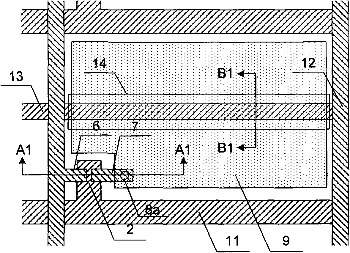
[0062] The technical solutions of the present invention will be described in further detail below with reference to the accompanying drawings and embodiments.

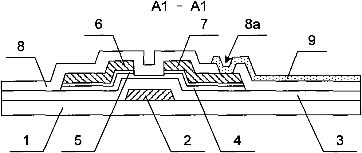
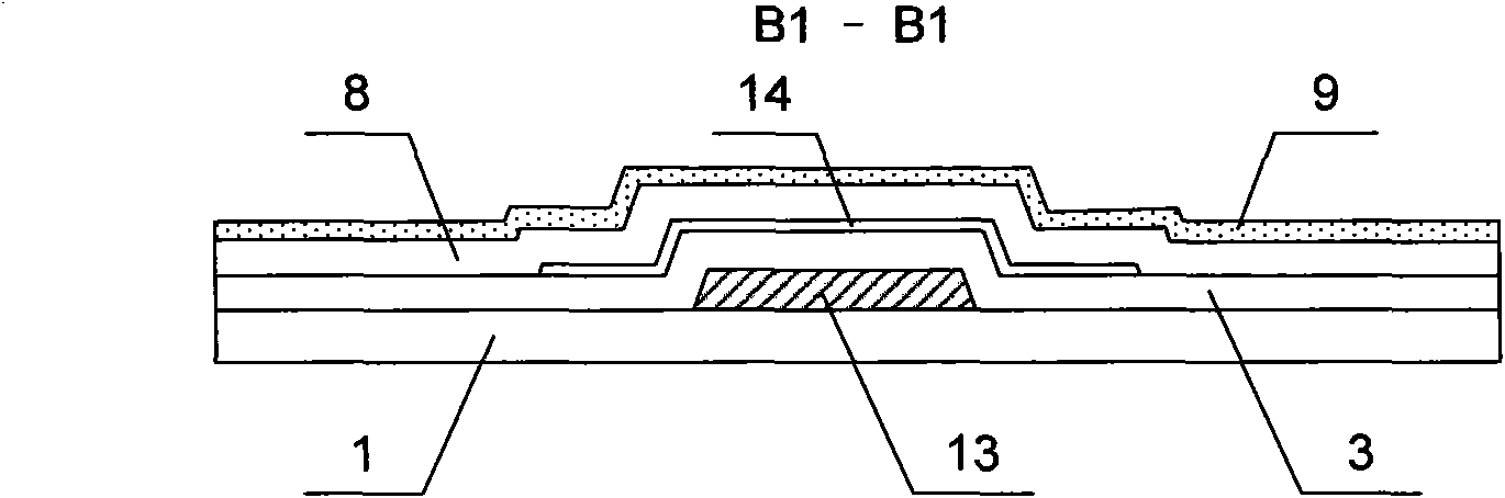
[0063] figure 1 It is a plan view of the first embodiment of the TFT-LCD array substrate of the present invention, reflecting the structure of a pixel unit, figure 2 for figure 1 The cross-sectional view of A1-A1 in the middle, image 3 for figure 1 Sectional view of B1-B1 direction in the middle. Such as Figure 1 ~ Figure 3 As shown, the TFT-LCD array substrate of this embodiment is a structure formed by four patterning processes. The main structure includes gate lines 11, data lines 12, common electrode lines 13, pixel electrodes 9 and thin film formed on the substrate 1. Transistors, gate lines 11 and data lines 12 perpendicular to each other define a pixel area, thin film transistors and pixel electrodes 9 are formed in the pixel area, gate lines 11 are used to provide turn-on signals to the thin film transi...


PUM


Abstract

The invention relates to a TFT-LCD array substrate and a making method thereof. The array substrate comprises a gate line, a data line, a thin film transistor, a pixel electrode and a common electrode line, wherein the gate line, the data line and the thin film transistor are formed on the substrate, and the pixel electrode and the common electrode line form a storage capacitor, a pulse electrodeis arranged between the common electrode line and the pixel electrode and is used for enabling the storage capacitor to have a first capacitance value when the pixel electrode is started to be charged and enabling the storage capacitor to have a second capacitance value when pixel electrode charging is finished, and the first capacitance value is smaller than the second capacitance value. In the invention, because the pulse electrode is arranged between the common electrode line and the pixel electrode, on the one hand, the storage capacitor has the smaller capacitance value when pixel electrode charging is started so as to lower load of the thin film transistor and enhance the charging capability of the thin film transistor, and on the other hand, the storage capacitor has the larger capacitance value when pixel electrode charging is finished to strengthen the holding property of voltage of the pixel electrode and lower the leaping voltage of the pixel electrode at the moment that the thin film transistor is closed.

Description

technical field [0001] The invention relates to a thin film transistor liquid crystal display and a manufacturing method thereof, in particular to a TFT-LCD array substrate and a manufacturing method thereof. Background technique [0002] Thin Film Transistor Liquid Crystal Display (TFT-LCD for short) is mainly composed of an array substrate and a color filter substrate that are boxed together and the liquid crystal is sandwiched between them. The array substrate is formed with matrix-arranged thin film transistors and Pixel electrodes, each pixel electrode is controlled by a thin film transistor, and the electric field between the two substrates is adjusted by charging and discharging the pixel electrode, so as to control the flipping of the liquid crystal to achieve the display effect. [0003] When the TFT-LCD is working, the pixel electrode is charged when the thin film transistor is turned on, and after the thin film transistor is turned off, the pixel electrode voltage...

Claims


Application Information

Patent Timeline
IPC IPC(8): G02F1/1362G02F1/1368H01L21/82
Inventor 马占洁
Owner BOE TECH GRP CO LTD
Why Eureka
Try Eureka