A charge storage type insulated gate bipolar transistor and a preparation method thereof

A bipolar transistor, charge storage technology, applied in semiconductor/solid-state device manufacturing, circuits, electrical components, etc., to achieve excellent device characteristics, improve concentration distribution, and change the band gap.

Active Publication Date: 2019-01-11
UNIV OF ELECTRONICS SCI & TECH OF CHINA
View PDF7 Cites 5 Cited by
  • Summary
  • Abstract
  • Description
  • Claims
  • Application Information

AI Technical Summary

Problems solved by technology

[0008] The present invention aims at the adverse effects of the doping concentration and thickness of the charge storage layer on the breakdown voltage of the device in the prior art, and limits the compromise between the breakdown voltage of the device, the forward conduction voltage drop and the turn-off loss, and provides An insulated gate bipolar transistor with a heterojunction charge storage layer, which bends the energy band by forming a homogeneous heterojunction in the charge storage layer, thereby introducing a minority carrier barrier on the side close to the drift region, thereby To improve the carrier concentration distribution in the drift region, so as to obtain a lower forward conduction voltage drop and a better trade-off relationship between forward conduction voltage drop and turn-off loss, and avoid increasing the concentration of the charge storage layer on device breakdown adverse effects of voltage

Method used


Image

  • A charge storage type insulated gate bipolar transistor and a preparation method thereof
  • A charge storage type insulated gate bipolar transistor and a preparation method thereof
  • A charge storage type insulated gate bipolar transistor and a preparation method thereof

Examples


Embodiment 1

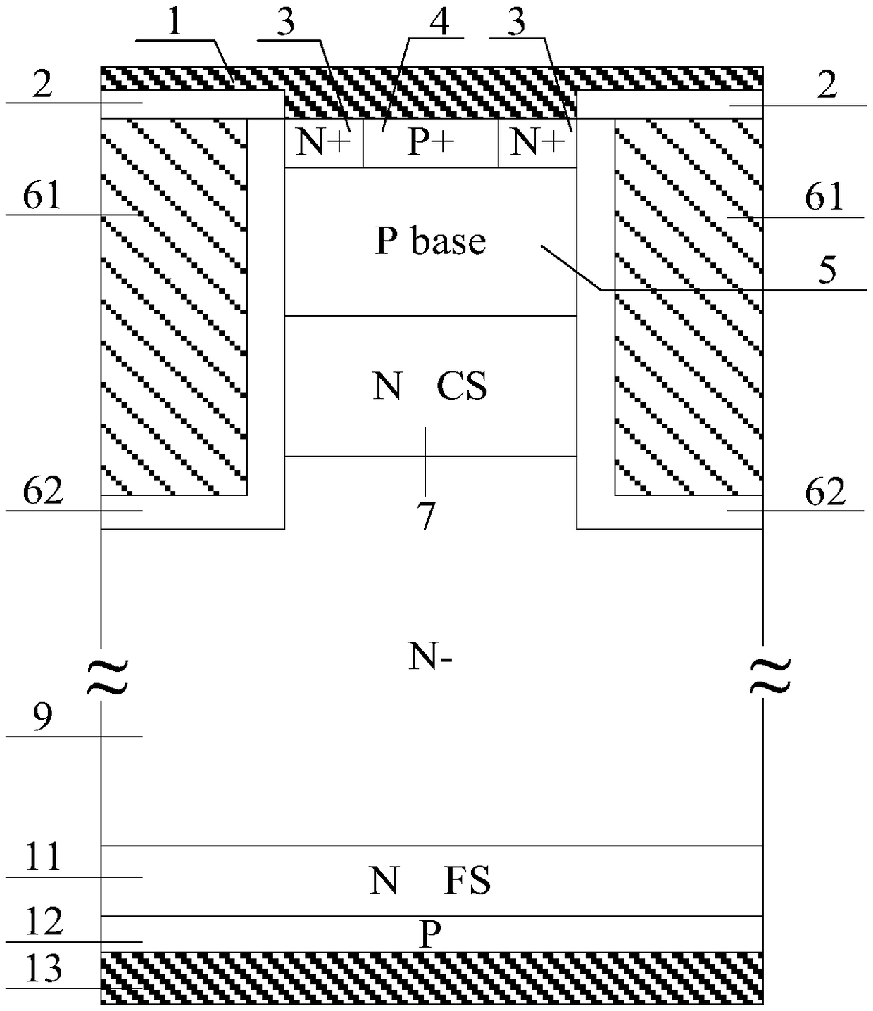
[0068] This embodiment provides a strained Si~Si 1-x Ge x Insulated gate bipolar transistor with homotype heterojunction charge storage layer, Figure 4 Its semi-cellular structure is shown, and its cellular structure includes: collector metal 13, P-type collector region 12, N-type field stop layer 11, N-drift region 9, N-type charge storage layer 7, P-type base Region 5, P+ emitter region 4, N+ emitter region 3, trench gate structure and emitter metal 1; collector metal 13 is arranged on the back of P-type collector region 12; N-type field stop layer 11 is arranged on P-type collector The front of the region 12; the N-type drift region 9 is arranged on the front of the N-type field stop layer 11; the P-type base region 5 is arranged on the top layer of the N-drift region 9; the P+ emitter region 4 is in contact with both sides of the P+ emitter region 4 The N+ emitter region 3 is arranged side by side on the top layer of the P-type base region 5; the N-type charge storage l...

Embodiment 2

[0075] This embodiment provides a strained Si~Si 1-x Ge x Insulated gate bipolar transistor with homotype heterojunction charge storage layer, Figure 11 Its semi-cellular structure is shown. In this embodiment, except that a P-type layer 10 with a junction depth of 0.5-1 μm is introduced at the bottom of the trench gate structure, other structures are the same as those in Embodiment 1.

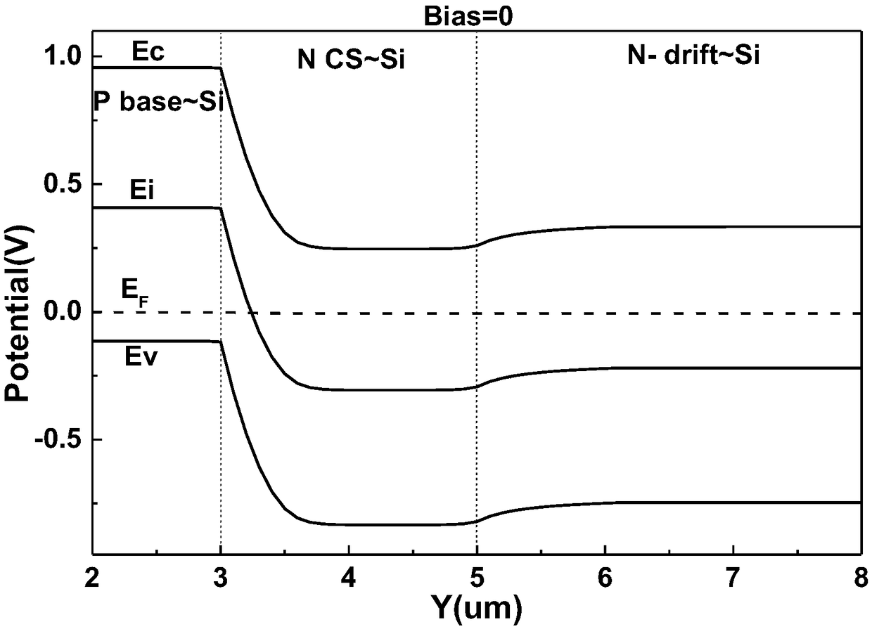
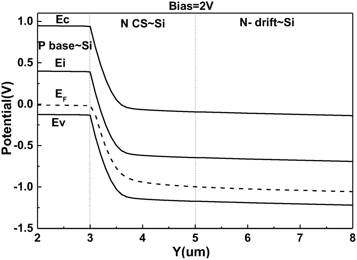
[0076] This embodiment introduces a P-type layer 10 connected to the gate electrode 61 through a gate dielectric layer 62, and the P-type layer 10 extends laterally to both sides into the N-drift region 9 below the heterojunction N-type charge storage layer 7, so as to This shields the influence of negative charges in the N-type charge storage layer 7, improves the concentration of the electric field at the bottom of the trench, and improves the breakdown voltage and reliability of the device.

Embodiment 3

[0078] This embodiment provides a strained Si~Si 1-x Ge x Insulated gate bipolar transistor with homotype heterojunction charge storage layer, Figure 12 Its semi-cellular structure is shown. In this embodiment, except that the split electrode 81 and the split electrode dielectric layer 82 are introduced into the trench gate structure 6 to form the split trench gate structure, the rest of the structure is the same as that of the embodiment 2.

[0079] The depth of the gate electrode 61 in the split trench gate structure is greater than the junction depth of the P-type base region 5 and smaller than the junction depth of the N-type charge storage layer 7; the depth of the split electrode 82 is greater than the junction depth of the N-type charge storage layer 7 deep; the split electrode 82 is connected to the gate electrode 61 through the gate dielectric layer 62, and is connected to the N-type charge storage layer 7 and the N-drift region 9 through the split electrode dielec...


PUM


Abstract

The invention relates to a charge storage type insulated gate bipolar transistor and a preparation method thereof, belonging to the technical field of power semiconductors. By improving the charge storage layer of the traditional charge storage type IGBT device, a semiconductor material used for the charge storage layer remote from the drift region has a larger band gap than a semiconductor material used for the charge storage layer close to the drift region, so that the semiconductor materials with different forbidden band widths form the same-type heterojunction at their contact interfaces,thereby forming a potential barrier that prevents minority carriers in the drift region from entering the base region. As a result, the carrier distribution concentration in the drift region is improved, the conductivity modulation effect of the IGBT is enhanced, the forward conduction voltage drop Vceon of the device is reduced, the breakdown voltage of the IGBT is optimized, and the tradeoff between the forward conduction voltage drop Vceon and the shutdown loss Eoff is achieved. Moreover, by adjusting the doping concentration of materials with different bandgap widths in the charge storagelayer and the combination of materials with different bandgap widths, the invention can further optimize the working characteristics of the device.

Description

technical field [0001] The invention belongs to the technical field of power semiconductor devices, and in particular relates to a charge storage type insulated gate bipolar transistor and a preparation method thereof. Background technique [0002] IGBT is a device composed of MOSFET (input stage) and PNP transistor (output stage). It not only has the characteristics of easy driving, low input impedance and fast switching speed of MOSFET devices, but also has the on-state current density of bipolar devices. Large, low conduction voltage, low loss, and good stability. Based on these excellent device characteristics, IGBT has become a mainstream power device widely used in medium and high voltage fields in recent years, such as high-speed rail, electric vehicles, motor drives, grid-connected technology, energy storage power stations, AC / DA conversion and frequency conversion speed regulation and other fields . The use of IGBT for power conversion can improve the efficiency a...

Claims


Application Information

Patent Timeline
Patent Type & Authority Applications(China)
IPC IPC(8): H01L29/06H01L21/335H01L29/739
CPCH01L29/0607H01L29/66348H01L29/7397
Inventor 张金平赵倩王康刘竞秀李泽宏张波
Owner UNIV OF ELECTRONICS SCI & TECH OF CHINA
Why Eureka
Try Eureka